Two-dimensional layer materials for highly efficient molecular sensing based on surface-enhanced Raman scattering
-
摘要: 表面增强拉曼散射(SERS)因其无损检测、快速响应和高灵敏度等优点,已经发展成为一种高效的分子探测技术。但目前大多数关于SERS的研究仍然基于贵金属材料(如Au、Ag等),成本高、表面均匀性较低、生物相容性差等不足限制了其广泛应用。石墨烯具有原料来源丰富、二维原子级平面、大比表面积、高稳定性和独特的电学和光学性能等优势,研究表明其可作为一种有效的SERS基底材料,为相关研究开拓了新思路。近年来,过渡金属硫族化合物(TMDCs)、六方氮化硼、黑磷、二维碳氮化物等二维无机层状材料也开始受到研究者关注。本文综述了石墨烯、TMDCs等二维层状材料作为SERS基底的最新研究进展并阐述了SERS增强机理。在此基础上,提出了二维层状材料用于高性能SERS基底材料研究面临的一些挑战,并对该领域发展前景进行了展望。Abstract: Surface-enhanced Raman scattering (SERS) has been regarded as an attractive technique for efficient molecular sensing because of its nondestructive detection, fast response and high sensitivity. However, the majority of studies on SERS are still based on noble metals (e.g. Au, Ag), which suffer from the drawbacks of high-cost, low uniformity and poor stability, thus limiting their widespread use. Graphene shows an efficient SERS performance because of its two-dimensional (2D) atomically flat surface, large specific surface area, high stability and unique electronic/optical properties, which open up new avenues for SERS research. In recent years, other 2D inorganic layer materials, such as transition metal dichalcogenides (TMDCs), hexagonal boron nitride (h-BN), black phosphorus (BP), and MXenes, have also attracted increasing research attention. We summarize the SERS mechanisms and state-of-the-art progress on substrates based on 2D materials, including graphene and other 2D inorganic layer materials. The challenges and prospects for future research on high-performance SERS substrates are considered.
-
Key words:
- Graphene /
- SERS /
- Enhancement mechanism /
- Molecular sensing
-

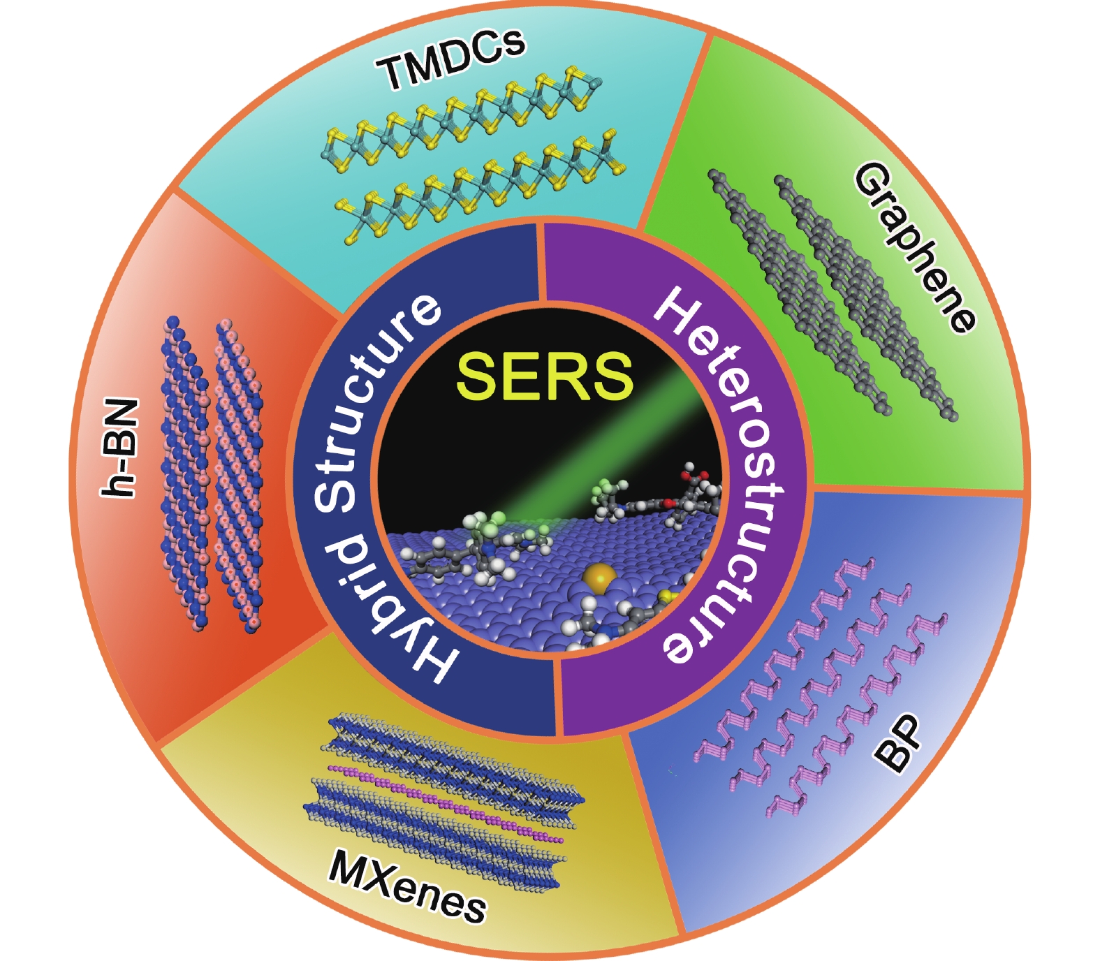
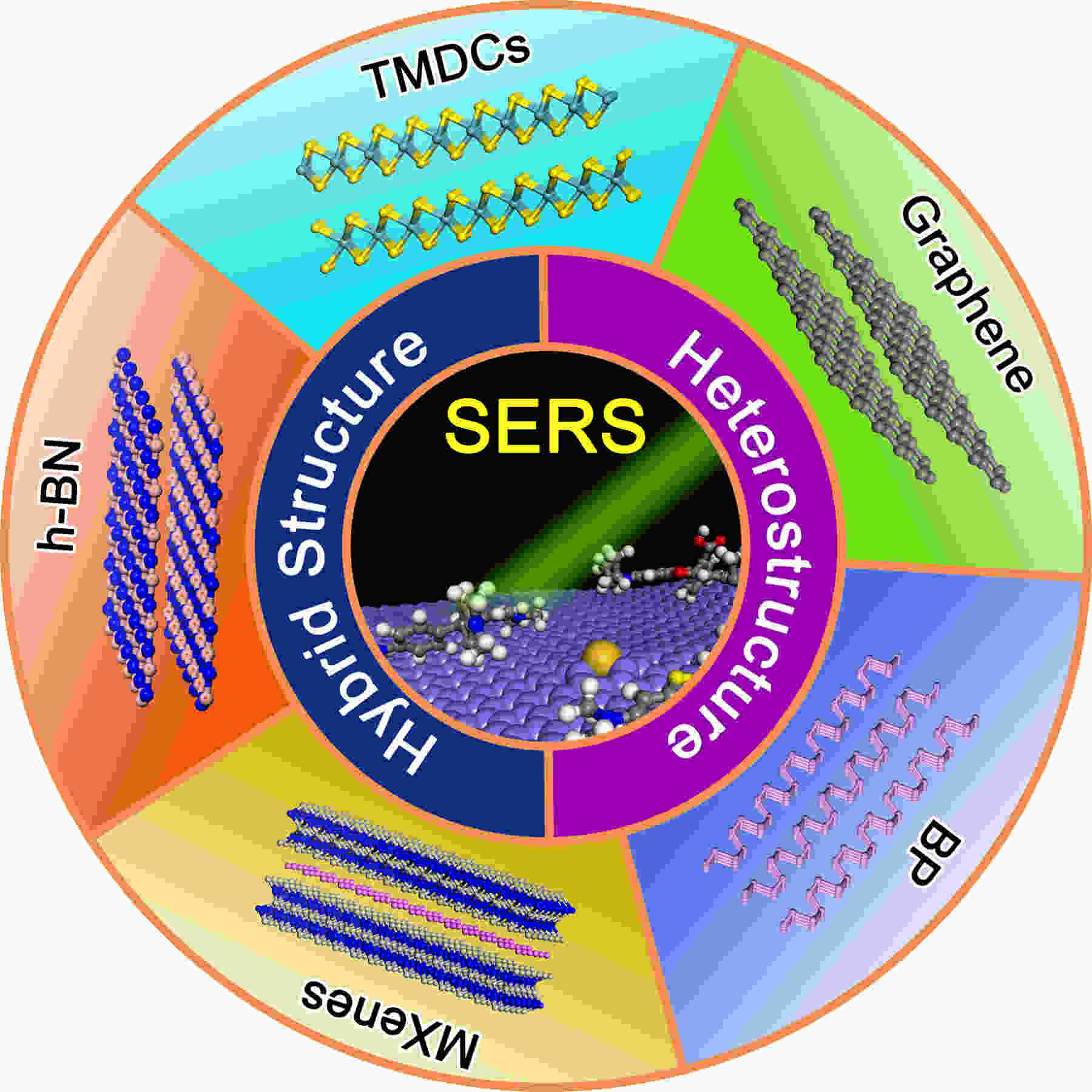
Figure 1. Various inorganic 2D layered materials for surface-enhanced Raman scattering (SERS). Here h-BN denotes hexagonal boron nitride. TMDCs and BP denote transition metal dichalcogenides and black phosphorus, respectively.

Figure 2. Schematic illustrations of (a) SERS, (b) mechanism of Raman scattering (ν0 and Δν represent the frequency of incident light and the change of frequencies after scattering, respectively), (c) electromagnetic mechanism (EM) and (d) chemical mechanism (CM) for SERS (Here E0 is the incident electromagnetic field, μmol is the induced dipole moment of probe molecule, r is the radius of the metal spheres and d is the distance between the probe molecule and the surface of metal sphere, CT represents the charge transfer, HOMO and LUMO denote the highest occupied molecular orbital and the lowest unoccupied molecular orbital, respectively).
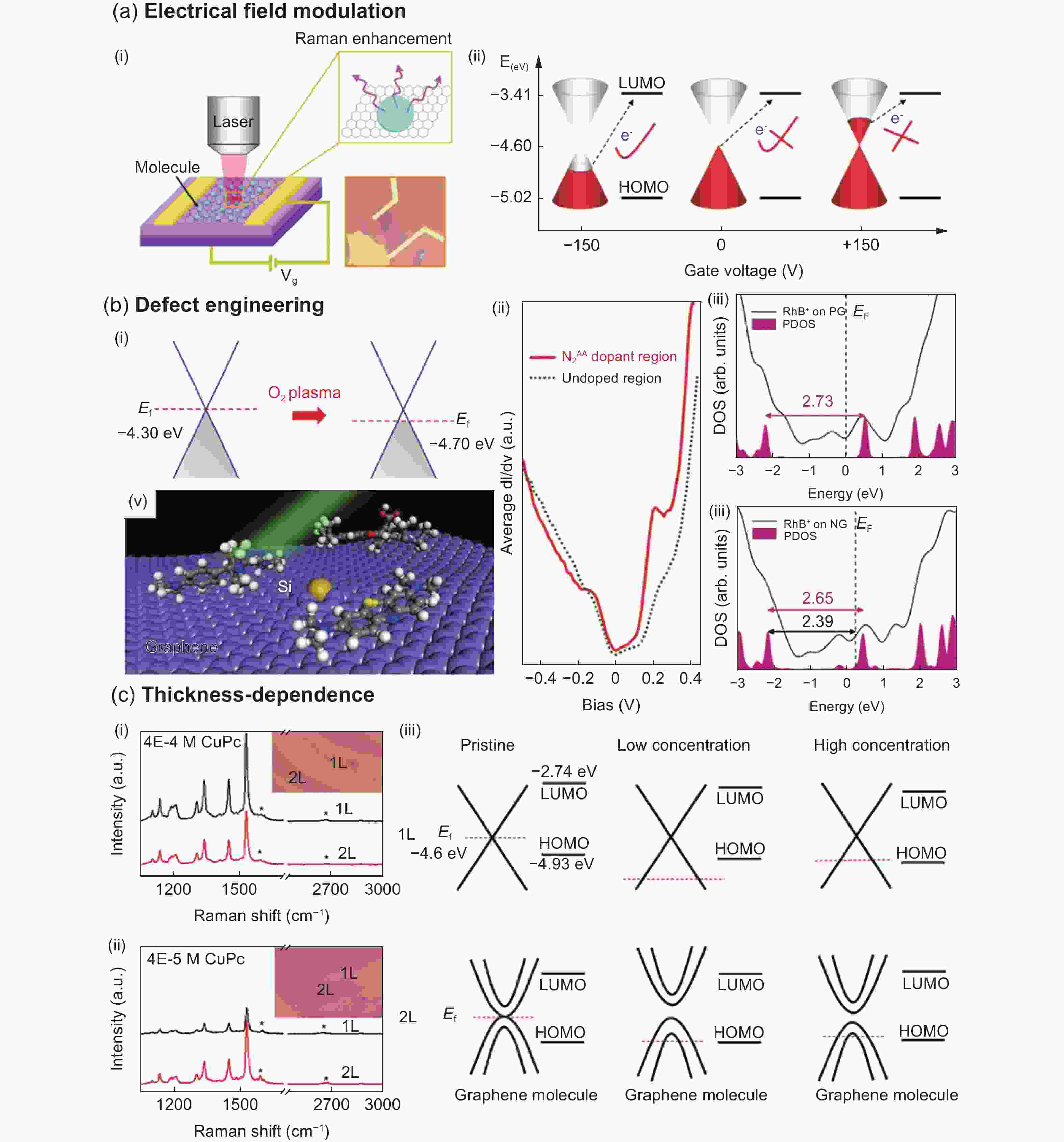
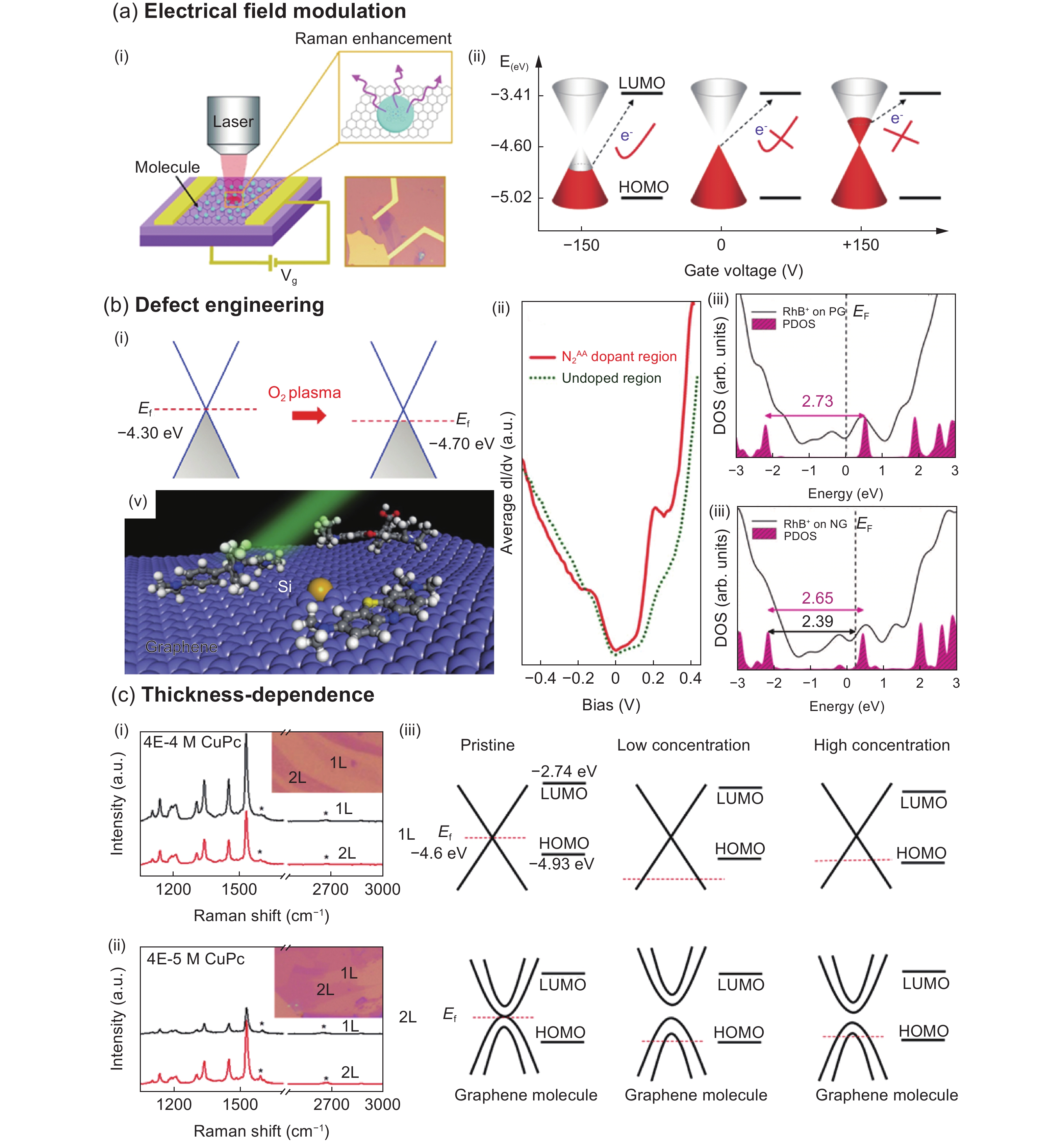
Figure 3. (a) Electrical field modulation on Fermi level for graphene-enhanced Raman scattering (GERS). (i) Schematic diagram of the device on tuning the graphene Fermi level by electrical field effect. (ii) The energy level alignment between the molecular energy level and modulated graphene Fermi level for charge transfer resonance[23] (reprinted with permission from American Chemical Society). (b) Defect engineering for GERS. (i) Schematic illustrations of the Fermi level modulation by O2 plasma treatment[33] (reprinted with permission from Elsevier). (ii) the dI/dV curves (averaged over 9 points spectra taken in 1×1 nm2 area) measured on N2AA dopants and undoped graphene[25] (reprinted with permission from Spring Nature). The density of states (DOS) for Rhodamine B (RhB) on (iii) the pristine graphene (PG) and (iv) N-doped graphene (NG), EF represents the Fermi level[14] (reprinted with permission from AAAS), (v) Schematic of SERS on Si-doped graphene[32] (reprinted with permission from John Wiley and Sons). (c) Thickness-dependence of GERS. (i-ii) Raman spectra of copper phthalocyanine (CuPc) molecule and (iii) schematic illustration of the energy band structure of mono- and bilayer graphene under low and high concentration molecular solution[36] (reprinted with permission from American Chemical Society).
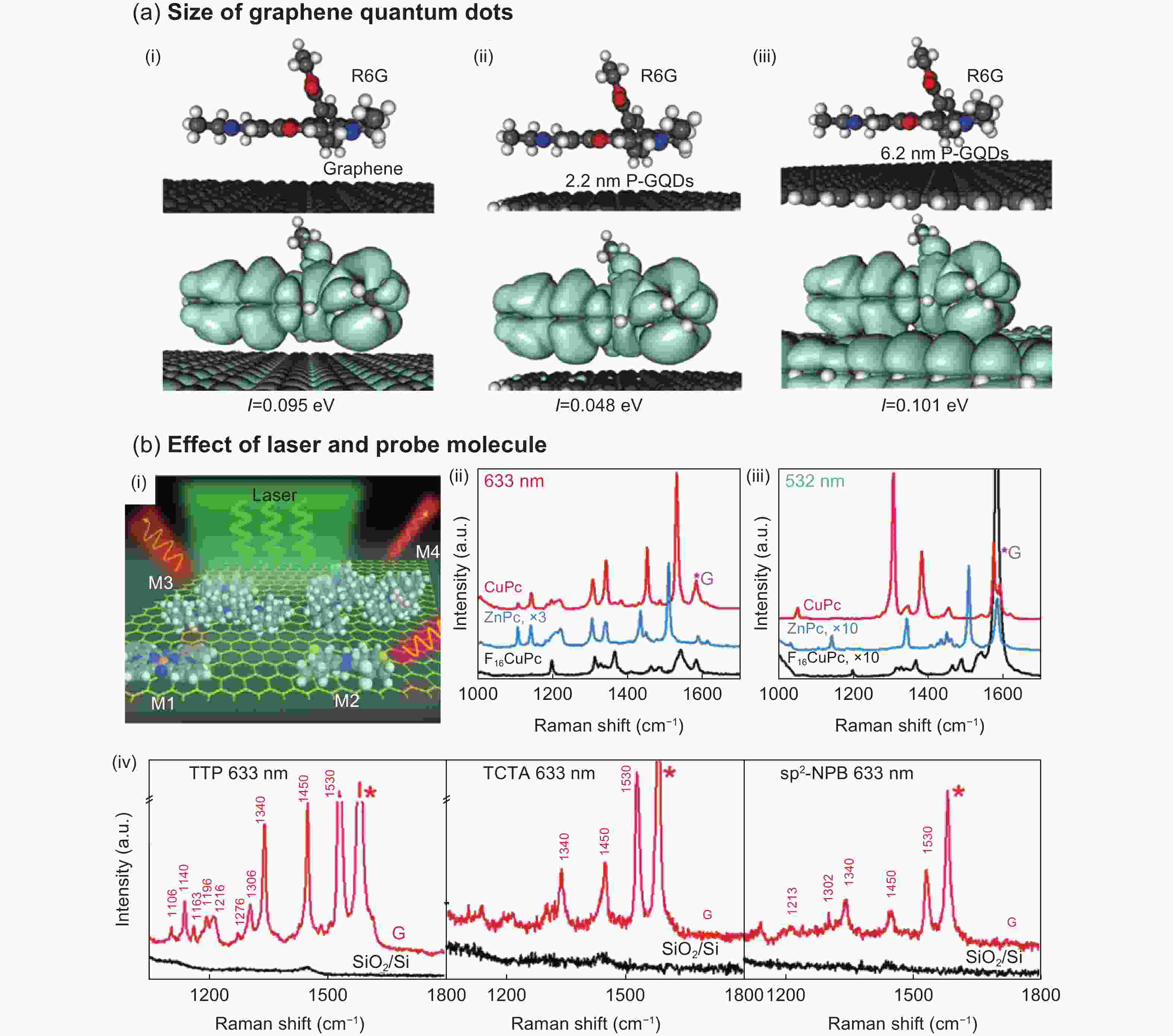
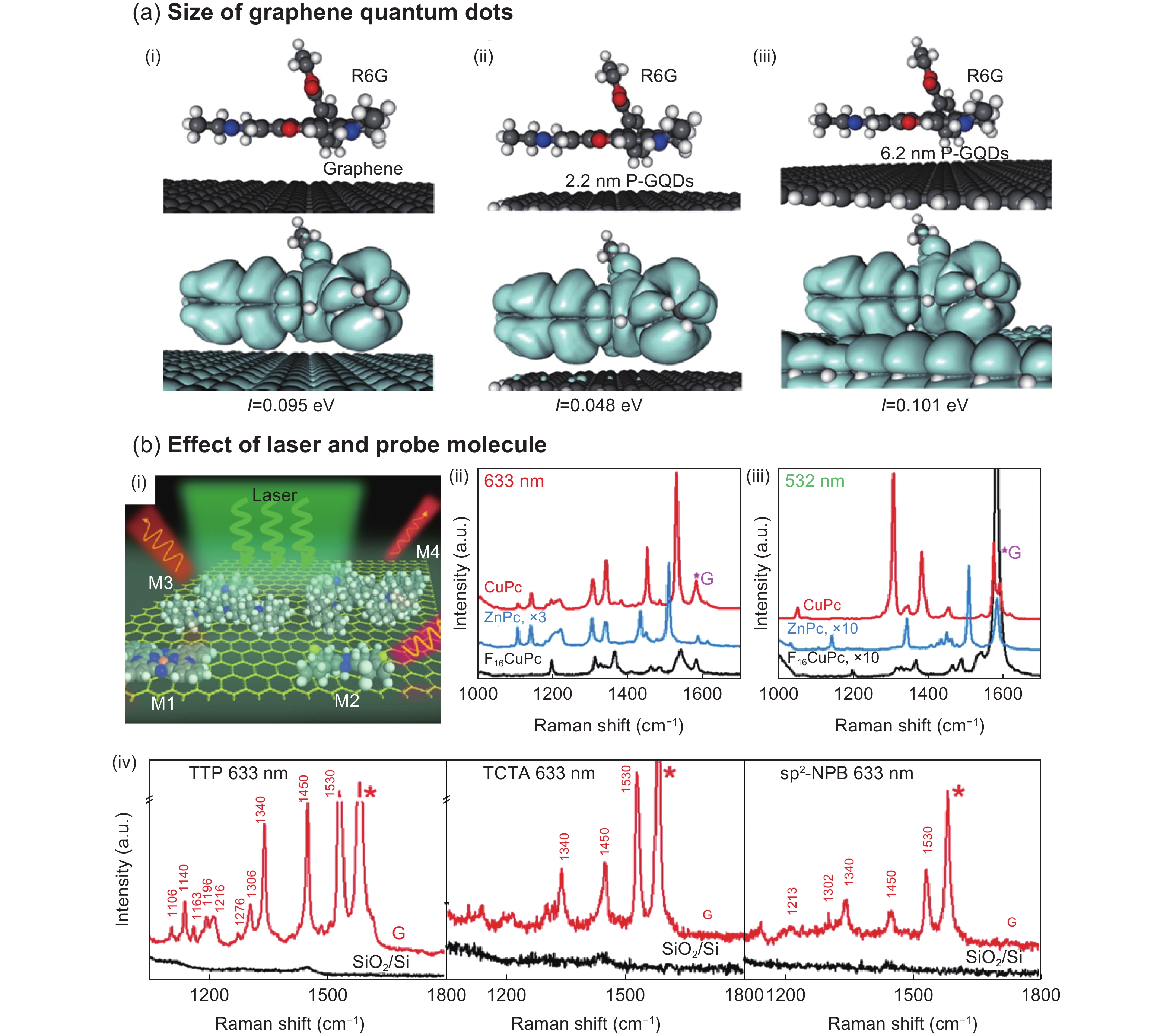
Figure 4. (a) The influence of size of graphene quantum dots on GERS. The calculated charge transfer integrals (I) of rhodamine 6G (R6G) with (i) pristine graphene and high-quality graphene quantum dots prepared by plasma-enhanced chemical vapor deposition (P-GQDs) of (ii) 2.2 nm and (iii) 6.2 nm sizes[39] (reprinted with permission from Spring Nature). (b) Impact of molecule and laser energy. (i) Schematic illustration of the influence of molecule and laser on GERS (here M1–M4 represent four different molecules). Raman spectra of CuPc, zinc phthalocyanine (ZnPc), and copper(II)1,2,3,4,8,9,10,11,15,16,17,18,22,23,24,25-hexadecafluoro-29H,31H-phthalocyanine (F16CuPc) under (ii) 532 nm and (iii) 633 nm laser. (iv) Raman spectra of tetrathienophenazine (TTP), tris(4-carbazoyl-9-ylphenyl) amine (TCTA), and 2,2′,7,7′-tetra(N-phenyl-1-naphthyl-amine)-9,9′-spirobifluorene (sp2-NPB) on graphene[40] (reprinted with permission from American Chemical Society).

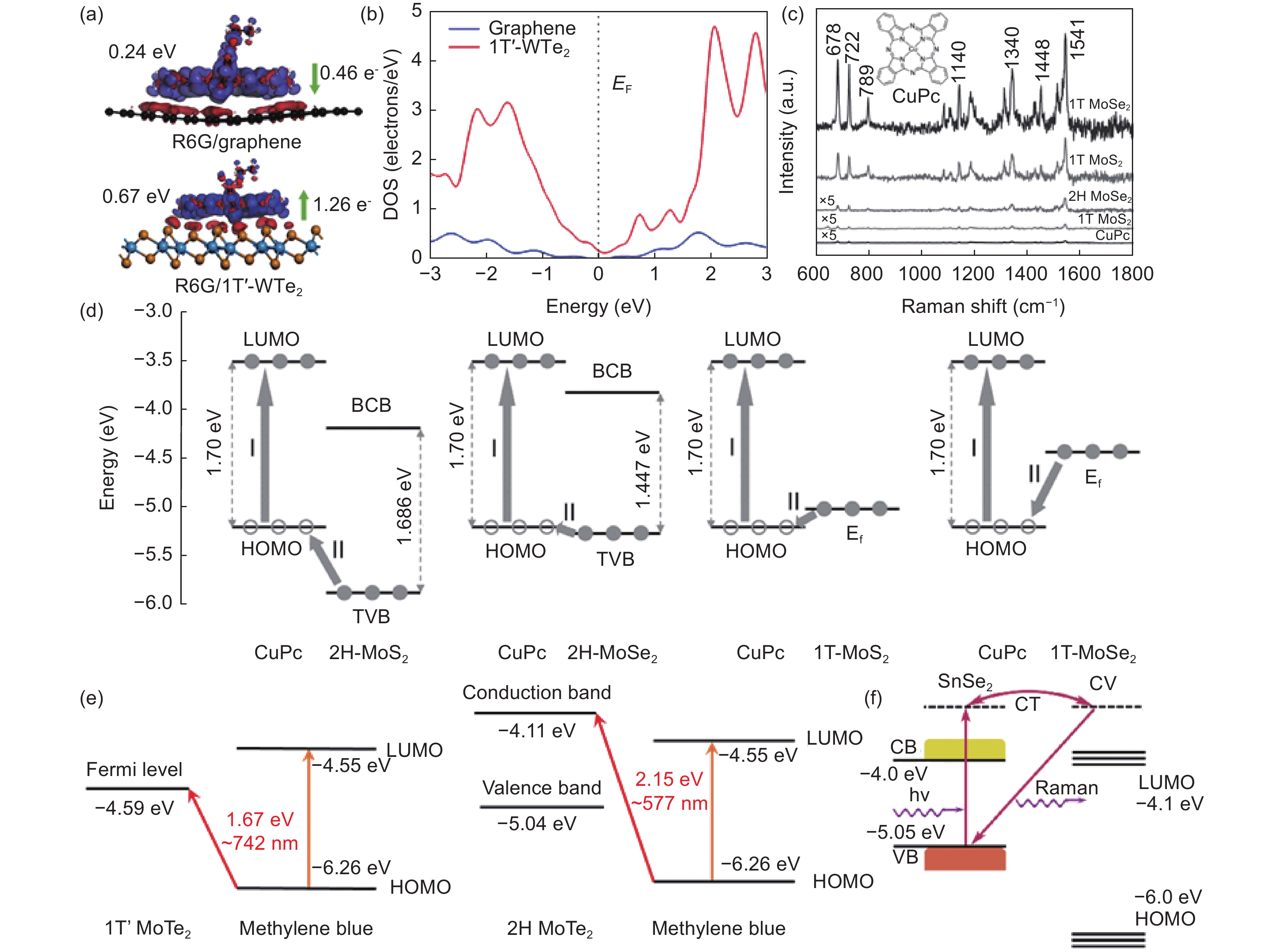
Figure 5. (a) The electron density difference isosurfaces for R6G on graphene and 1T’-WTe2. (b) DOS of 1T’-WTe2 and graphene [46] (reprinted with permission from American Chemical Society). (c) SERS spectra and (d) schematic illustration of charge transfer mechanism of CuPc on different substrates[21] (reprinted with permission from John Wiley and Sons). (e) Schematic illustration of energy level and charge transfer resonance process for SERS of MB on 1T’- and 2H MoTe2[50] (reprinted with permission from IOP). (f) Schematic illustration of energy level and charge transfer process for SERS of crystal violet (CV) on SnSe2[52] (reprinted with permission from John Wiley and Sons).

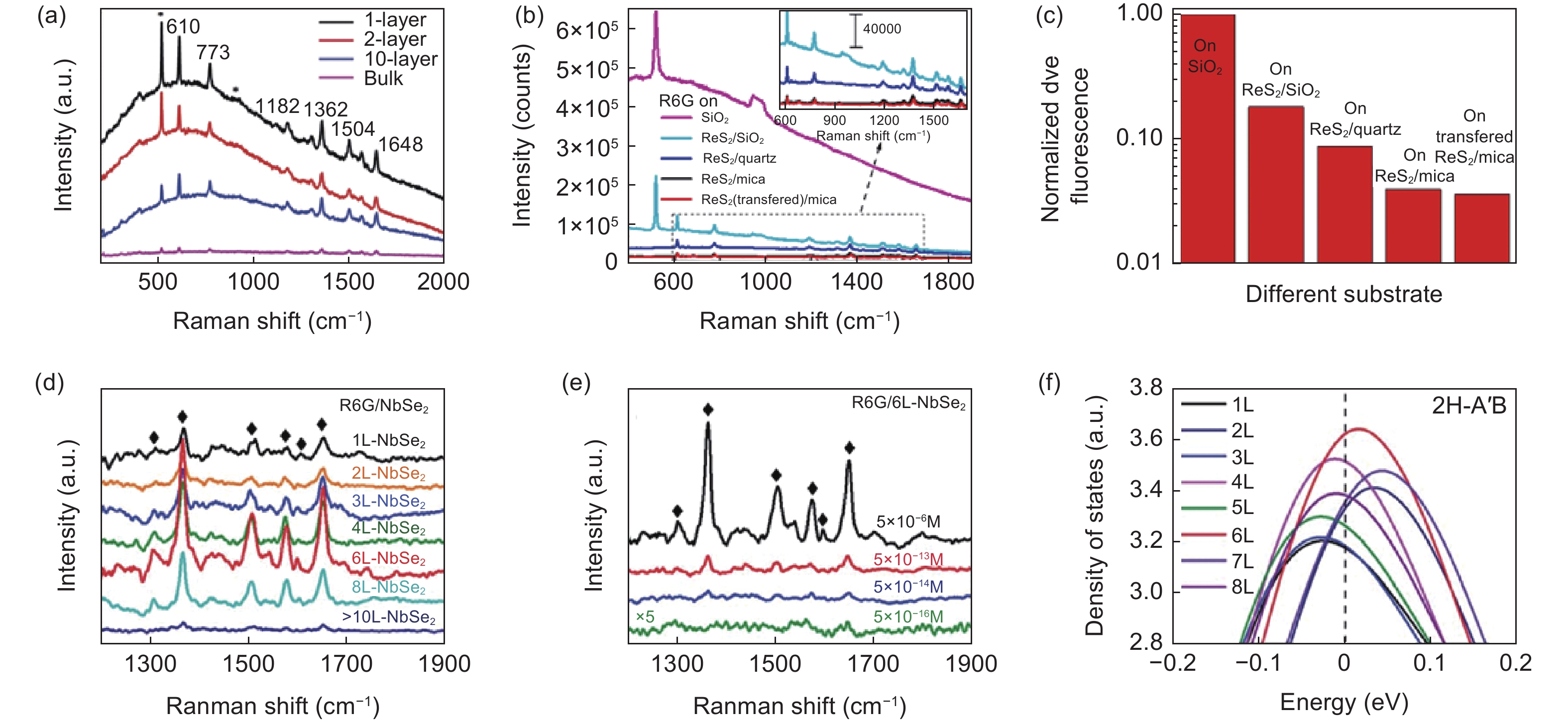
Figure 6. (a) SERS spectra of 10−6 mol L−1 R6G on different layer number ReS2 films[55] (reprinted with permission from John Wiley and Sons). (b-c) SERS spectra and normalized fluorescence of R6G on monolayer ReS2 with different underlying substrates[56] (reprinted with permission from Elsevier). SERS spectra of R6G (d) with 5×10⁻⁶ mol L−1 on NbSe2 with different layer numbers and (e) on 6L-NbSe2 with different R6G concentrations. (f) DOS of the outermost layer of 2H-NbSe2 with different layers in the A’B stacking mode[57] (reprinted with permission from Royal Society of Chemistry).
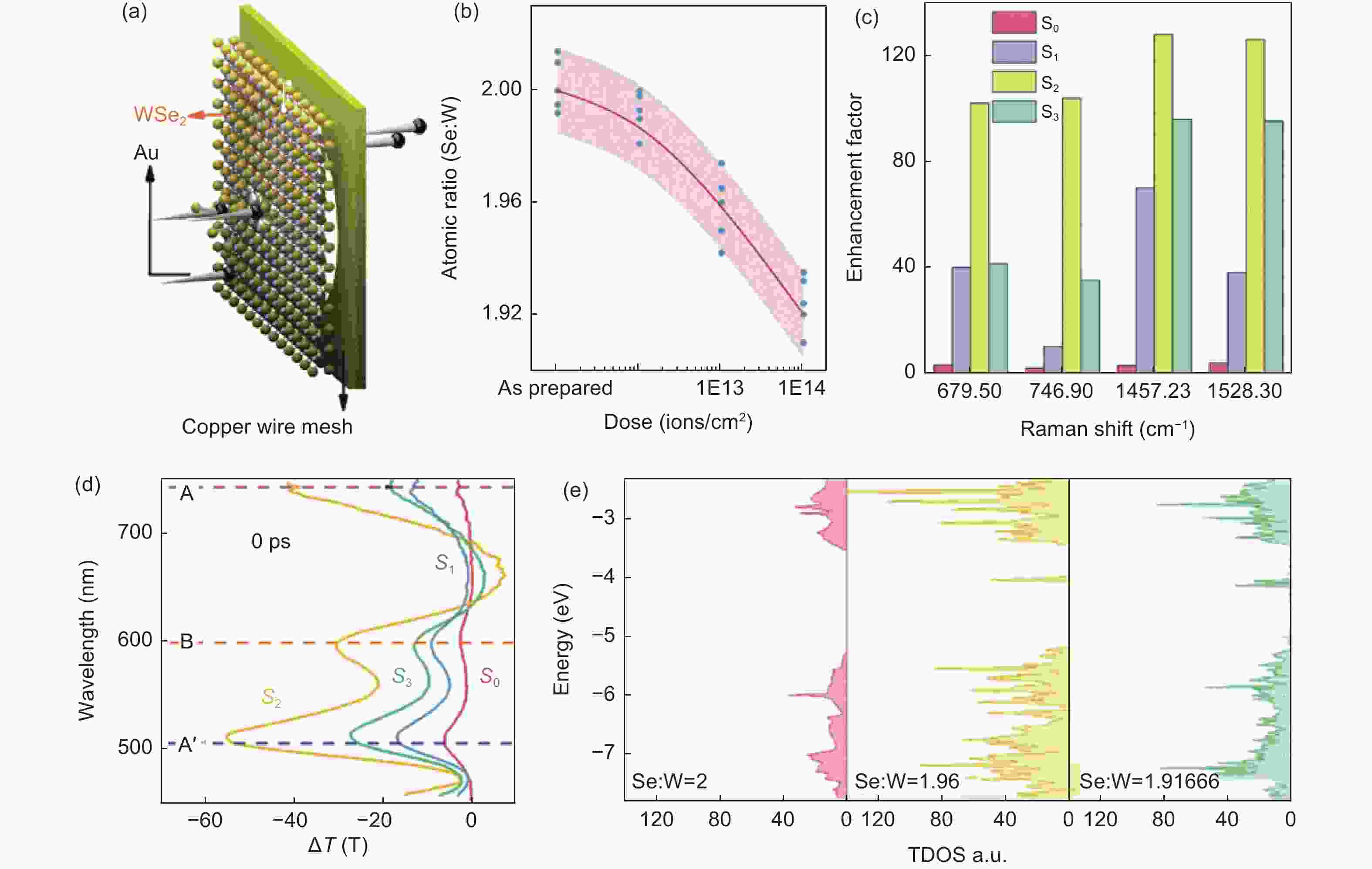
Figure 7. (a) Schematic diagram of Au ion irradiation. (b) Evolution of atomic ratio of WSe2 with the influence of incident ions. (c) The enhancement factor (EF) of SERS for CuPc on pristine (S0) and irradiated WSe2 monolayers by different controlled dose/fluence (S1=1012 ions cm−2, S2=1013 ions cm−2, S3=1014 ions cm−2) of ion beam. (d) The intensity of fs optical pump-probe spectroscopy at the wavelengths of 510 nm (A’), 596 nm (B) and 744 nm (A) at a time of 0 ps. (e) The total density of states (TDOS) of WSe2 with various atomic ratios[44] (reprinted with permission from John Wiley and Sons).

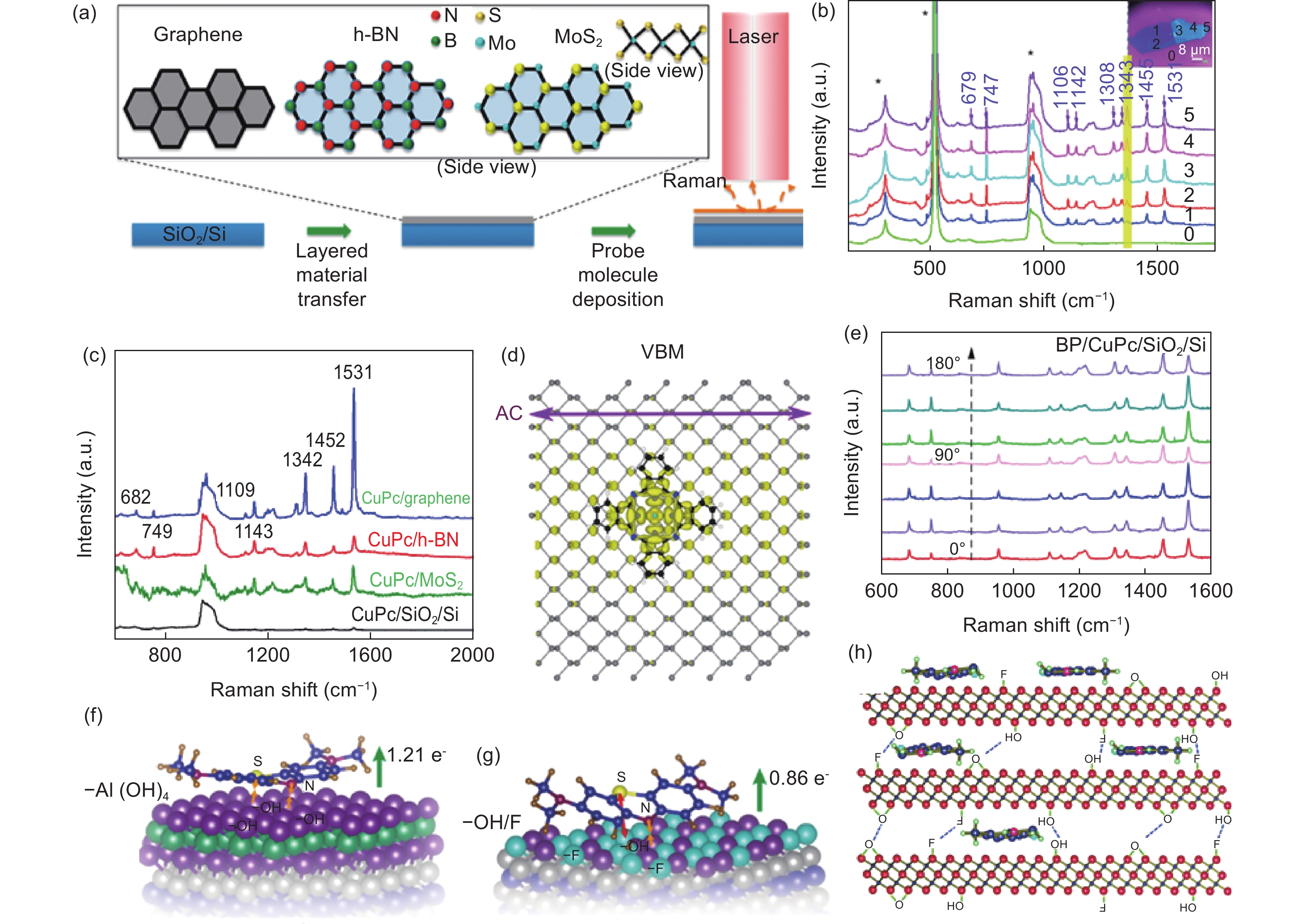
Figure 8. (a) Schematic illustration of graphene, h-BN and MoS2 served as SERS substrates. SERS spectra of CuPc on (b) different substrates and (c) h-BN flakes with various thicknesses[22] (reprinted with permission from American Chemical Society). (d) Charge distribution of valence band for CuPc/black phosphorus (BP) (here AC denotes armchair direction). (e) SERS spectra of CuPc on SiO2/Si with BP[65] (reprinted with permission from American Chemical Society). Schematic illustration of charge transfer on (f) methylene blue (MB)/Ti3C2-Al(OH)4 and (g) MB/Ti3C2-OH/F[70] (reprinted with permission from American Chemical Society). (h) Schematic of the adsorption and intercalation of MB in the MXene nanosheets[71] (reprinted with permission from AIP).

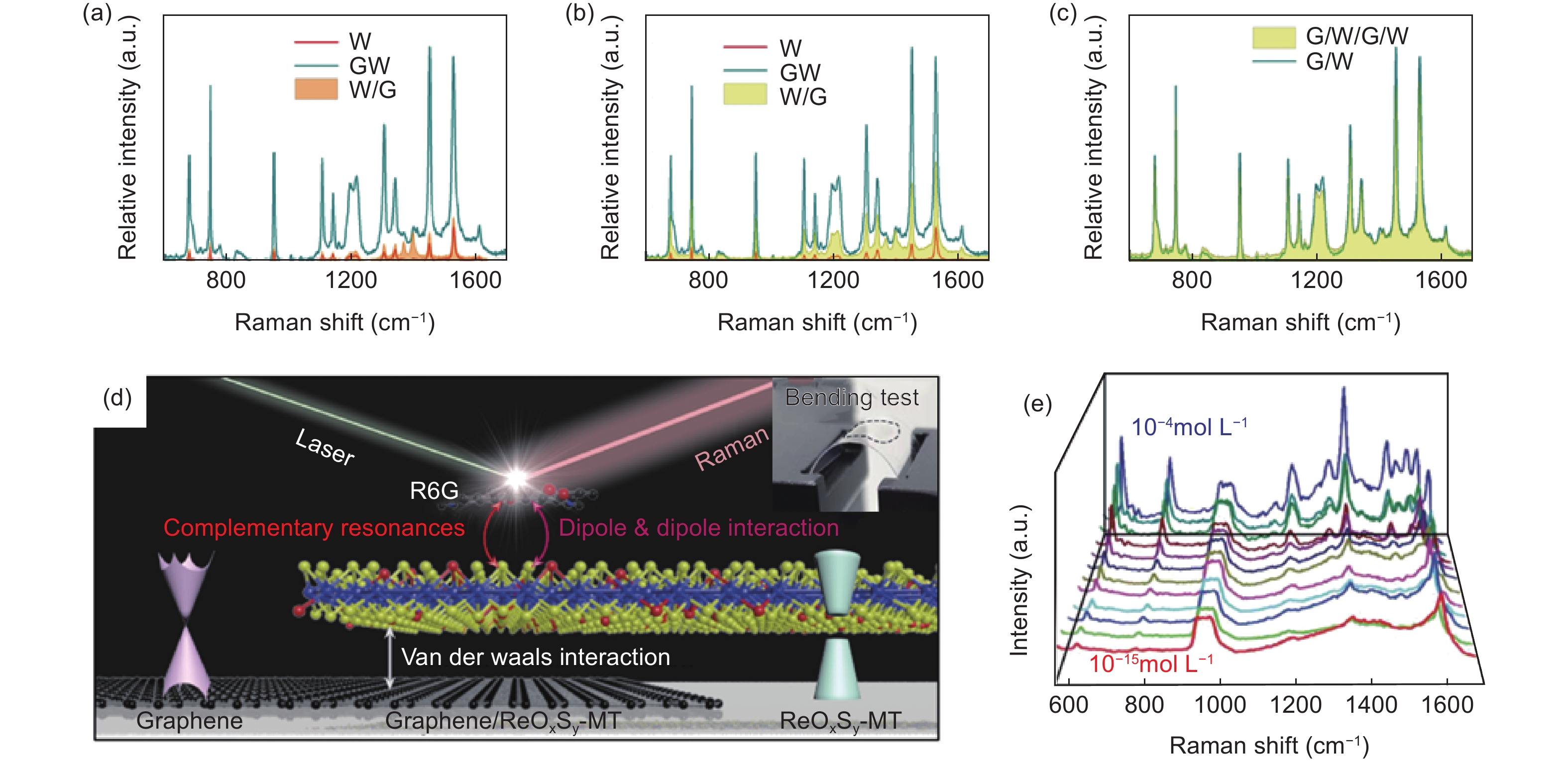
Figure 9. (a-c) SERS spectra of CuPc on different heterostucture substrates[72] (reprinted with permission from American Chemical Society). (d) Schematic of SERS effect on graphene/ReOxSy heterostructure and bending test. (e) SERS spectra of R6G on graphene/ReOxSy vertical heterostructure[73] (reprinted with permission from American Chemical Society).
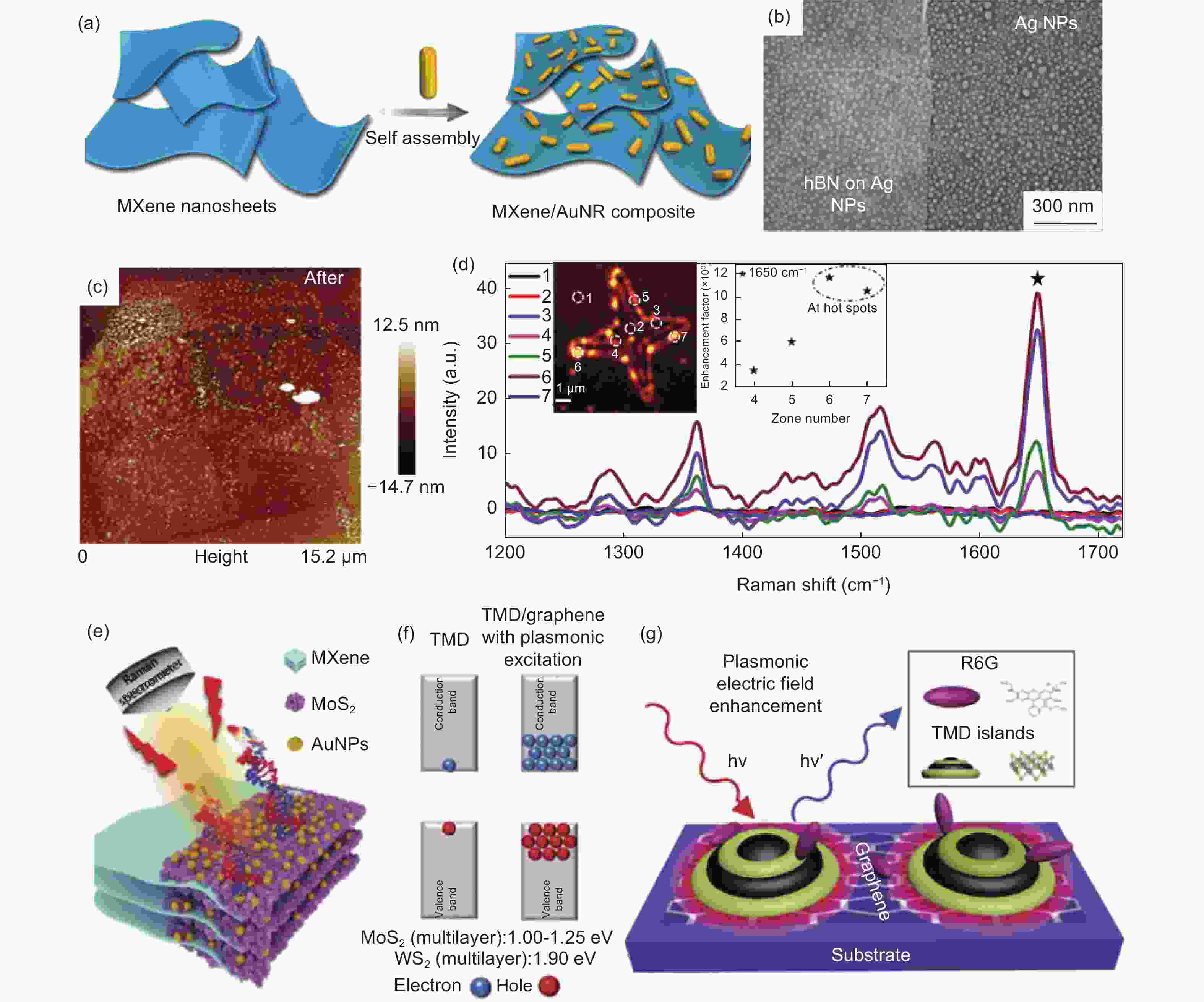
Figure 10. (a) Schematic diagram of the fabrication of the MXene/Au nanorods (AuNRs)[4] (reprinted with permission from American Chemical Society). (b) SEM image of Ag nanoparticles (AgNPs) covered by h-BN sample[78] (reprinted with permission from John Wiley and Sons). (c) AFM topography image of laser-etched MoS2 after decorated with AuNPs. (d) SERS spectra of RhB on various positions of AuNPs/MoS2[81] (reprinted with permission from American Chemical Society). (e) Schematic of MXene/MoS2@AuNPs for miRNA detection[82]. Schematic of (f) electron–hole pairs and (g) SERS mechanism of few-layer TMDs/graphene heterostructure[83] (reprinted with permission from John Wiley and Sons).
Table 1. SERS performances and related mechanisms of various 2D materials.
Substrate Probe
moleculeLaser wavelength
(nm)Limit of detection
(mol L−1)Mechanism Refs. Graphene CuPc 633 4×10⁻⁶ Charge transfer
(thickness-dependence)[36] Electrical field modulated graphene CoPc 633 <10−6 [23] Graphene quantum dots R6G 532 1×10⁻⁹ [39] O2 plasma treated graphene RhB 514 1×10⁻⁷ Local dipole and charge transfer
(thickness-dependence)[33] N-doped graphene RhB 514 5×10⁻¹¹ [14] WS2 R6G 532 1×10⁻⁷ Charge transfer and dipole-dipole interaction
(thickness-dependence)[53] ReS2 R6G 532 1×10⁻⁹ [55] 2H-MoS(Se)2 R6G 532 1×10⁻⁵ [21] 1T-MoS(Se)2 R6G 532 1×10⁻⁸ [21] 1T’-MoTe2 R6G 532 4×10⁻¹⁴ [46] 1T’-WTe2 R6G 532 4×10⁻¹⁵ [46] NbS2 MB 633 1×10⁻¹⁴ [54] NbSe2 R6G 532 5×10⁻¹⁶ [57] SnSe2 R6G 532 1×10⁻¹⁷ [51] Hexagonal boron nitride CuPc 633 Close to graphene Dipole-dipole interaction
(thickness-independence)[22] Ti3C2Tx MB 633 1×10⁻¹² Charge transfer (thickness-dependence) [70] Black phosphorus with nano-void array CuPc 532 1×10⁻⁸ Charge transfer (angle-dependence) [66] Graphene/ReOxSy R6G 532 1×10⁻¹⁵ Charge transfer and dipole-dipole interaction [73] Au nanoparticles/rGO R6G 633 1×10⁻⁸ Chemical mechanism and
electromagnetic mechanism[77] Wrinkled graphene/Au nanoparticles R6G 633 1×10⁻⁹ [85] MXene/Au nanorods R6G 532 1×10⁻¹² [4] Au nanoparticles/MoS2 RhB 532 1×10⁻¹⁰ [81] Mo(W)S2 nanodomes/graphene R6G 532 5×10⁻¹² [83] WS2+MoS2 nanodisks/graphene R6G 532 5×10⁻¹³ [84]  下载: 导出CSV
-
[1] Raman C V, Krishnan K S. A new type of secondary radiation[J]. Nature,1928,121:501-502. [2] Fleischmann M, Hendra P J, McQuillan A J. Raman spectra of pyridine adsorbed at a silver electrode[J]. Chemical Physics Letters,1974,26(2):163-166. doi: 10.1016/0009-2614(74)85388-1 [3] Zhu C, Zhao Q, Wang X, et al. Ag-nanocubes/graphene-oxide/Au-nanoparticles composite film with highly dense plasmonic hotspots for surface-enhanced Raman scattering detection of pesticide[J]. Microchemical Journal,2021,165:106090. doi: 10.1016/j.microc.2021.106090 [4] Xie H, Li P, Shao J, et al. Electrostatic self-assembly of Ti3C2Tx MXene and gold nanorods as an efficient surface-enhanced Raman scattering platform for reliable and high-sensitivity determination of organic pollutants[J]. ACS Sensors,2019,4(9):2303-2310. doi: 10.1021/acssensors.9b00778 [5] Li J, Koo K M, Wang Y, et al. Native microRNA targets trigger self-assembly of nanozyme-patterned hollowed nanocuboids with optimal interparticle gaps for plasmonic-activated cancer detection[J]. Small,2019,15(50):1904689. doi: 10.1002/smll.201904689 [6] Fraser J P, Postnikov P, Miliutina E, et al. Application of a 2D molybdenum telluride in SERS detection of biorelevant molecules[J]. ACS Applied Materials & Interfaces,2020,12(42):47774-47783. [7] Kim N, Thomas M R, Bergholt M S, et al. Surface enhanced Raman scattering artificial nose for high dimensionality fingerprinting[J]. Nature Communications,2020,11(1):207. doi: 10.1038/s41467-019-13615-2 [8] Kneipp K, Wang Y, Kneipp H, et al. Single molecule detection using surface-enhanced Raman scattering (SERS)[J]. Physical Review Letters,1997,78(9):1667-1670. doi: 10.1103/PhysRevLett.78.1667 [9] Zheng T, Zhou Y, Feng E, et al. Surface-enhanced Raman scattering on 2D Nanomaterials: Recent developments and applications[J]. Chinese Journal of Chemistry,2021,39(3):745-756. doi: 10.1002/cjoc.202000453 [10] Kannan P K, Shankar P, Blackman C, et al. Recent advances in 2D inorganic nanomaterials for SERS sensing[J]. Advanced Materials,2019,31(34):1803432. doi: 10.1002/adma.201803432 [11] Zhang N, Tong L, Zhang J. Graphene-based enhanced Raman scattering toward analytical applications[J]. Chemistry of Materials,2016,28(18):6426-6435. doi: 10.1021/acs.chemmater.6b02925 [12] Liebel M, Pazos-Perez N, Hulst N F, et al. Surface-enhanced Raman scattering holography[J]. Nature Nanotechnology,2020,15(12):1005-1011. doi: 10.1038/s41565-020-0771-9 [13] Qiu H, Wang M, Zhang L, et al. Wrinkled 2H-phase MoS2 sheet decorated with graphene-microflowers for ultrasensitive molecular sensing by plasmon-free SERS enhancement[J]. Sensors and Actuators B:Chemical,2020,320:128445. doi: 10.1016/j.snb.2020.128445 [14] Feng S, Fantos M C, Carvalho B R, et al. Ultrasensitive molecular sensor using N-doped graphene through enhanced Raman scattering[J]. Science Advances,2016,2(7):e1600322. doi: 10.1126/sciadv.1600322 [15] Smith E, Dent G. Modern Raman Spectroscopy: A Practical Approach [M]. England: Blackwell Science Publ, 2013. [16] Sebastian S. Surface-enhanced Raman spectroscopy: concepts and chemical applications[J]. Angewandte Chemie-International Edition,2014,53(19):4756-4795. doi: 10.1002/anie.201205748 [17] Laing S, Jamieson L E, Faulds K, et al. Surface-enhanced Raman spectroscopy for in vivo biosensing[J]. Nature Review Chemistry,2017,1(8):60. doi: 10.1038/s41570-017-0060 [18] Asing, Ali M E, Hamid S B A. SERS-modeling in molecular sensing[J]. Advanced Materials Research,2015,1109:223-226. doi: 10.4028/www.scientific.net/AMR.1109.223 [19] Judith L, Jimenez A D, Javier A, et al. Present and future of surface-enhanced Raman scattering[J]. ACS Nano,2020,14(1):28-117. doi: 10.1021/acsnano.9b04224 [20] Fukui K, Kato H, Yonezawa T. A molecular orbital theory of reactivity in aromatic hydrocarbons[J]. Journal of Chemical Physics,1952,20(4):722-725. doi: 10.1063/1.1700523 [21] Yin Y, Miao P, Zhang Y, et al. Significantly increased Raman enhancement on MoX2 (X = S, Se) monolayers upon phase transition[J]. Advanced Functional Materials,2017,27(16):1606694. doi: 10.1002/adfm.201606694 [22] Ling X, Fang W, Lee Y-H, et al. Raman enhancement effect on two-dimensional layered materials: graphene, h-BN and MoS2[J]. Nano Letters,2014,14(6):3033-3040. doi: 10.1021/nl404610c [23] Xu H, Xie L, Zhang H, et al. Effect of graphene Fermi level on the Raman scattering intensity of molecules on graphene[J]. ACS Nano,2011,5(7):5338-5344. doi: 10.1021/nn103237x [24] Marini A, Silveiro I, Javier Garcia de Abajo F. Molecular sensing with tunable graphene plasmons[J]. ACS Photonics,2015,2(7):876-882. doi: 10.1021/acsphotonics.5b00067 [25] Lv R, Li Q, Botello-Mendez A R, et al. Nitrogen-doped graphene: beyond single substitution and enhanced molecular sensing[J]. Scientific Reports,2012,2:586. doi: 10.1038/srep00586 [26] Novoselov K S, Geim A K, Morozov S V, et al. Electric field effect in atomically thin carbon films[J]. Science,2004,306(5696):666-669. doi: 10.1126/science.1102896 [27] Castro Neto A H, Guinea F, Peres N M R. The electronic properties of graphene[J]. Review of Modern Physics,2009,81(1):109-162. doi: 10.1103/RevModPhys.81.109 [28] Chung C, Kim Y-K, Shin D, et al. Biomedical applications of graphene and graphene oxide[J]. Accounts of Chemical Research,2013,46(10):2211-2224. doi: 10.1021/ar300159f [29] Paillet M, Parret R, Sauvajol J-L, et al. Graphene and related 2D materials: An overview of the Raman studies[J]. Journal of Raman Spectroscopy,2018,49(1):8-12. doi: 10.1002/jrs.5295 [30] Ling X, Xie L, Fang, Y, et al. Can graphene be used as a substrate for Raman enhancement[J]. Nano Letters,2010,10(2):553-561. doi: 10.1021/nl903414x [31] Ling X, Moura, L G, Pimenta M A, et al. Charge-transfer mechanism in graphene-enhanced Raman scattering[J]. Journal of Physical Chemistry,2012,116(47):25112-25118. [32] Lv R, dos Santos M C, Antonelli C, et al. Large-area Si-doped graphene: controllable synthesis and enhanced molecular sensing[J]. Advanced Materials,2014,26(45):7593-7599. doi: 10.1002/adma.201403537 [33] Mao H, Wang R, Zhong J, et al. Mildly O2 plasma treated CVD graphene as a promising platform for molecular sensing[J]. Carbon,2014,76:212-219. doi: 10.1016/j.carbon.2014.04.070 [34] Lv R, Terrones M. Towards new graphene materials: Doped graphene sheets and nanoribbons[J]. Materials Letters,2012,78:209-218. doi: 10.1016/j.matlet.2012.04.033 [35] Feng S, Lin, Z, Gan X, et al. Doping two-dimensional materials: ultra-sensitive sensors, band gap tuning and ferromagnetic monolayers[J]. Nanoscale Horizons,2017,2(2):72-80. doi: 10.1039/C6NH00192K [36] Ling X, Wu J, Xie L, et al. Graphene-thickness-dependent graphene-enhanced Raman scattering[J]. Journal of Physical Chemistry,2013,117(5):2369-2376. [37] Mercedes Messina M, Lorena Picone A, dos Santos Claro P C, et al. Graphene grown on Ni foam: molecular sensing, graphene enhanced Raman scattering, and galvanic exchange for surface enhanced Raman scattering applications[J]. Journal of Physical Chemistry,2018,122(16):9152-9161. [38] Zheng X, Peng Y, Yang, Y, et al. Hydrothermal reduction of graphene oxide; effect on surface-enhanced Raman scattering[J]. Journal of Raman Spectroscopy,2017,48(1):97-103. doi: 10.1002/jrs.4998 [39] Liu D, Chen X, Hu Y, et al. Raman enhancement on ultra-clean graphene quantum dots produced by quasi-equilibrium plasma-enhanced chemical vapor deposition[J]. Nature Communications,2018,9:193. doi: 10.1038/s41467-017-02627-5 [40] Huang S, Ling X, Liang L, et al. Molecular selectivity of graphene-enhanced Raman scattering[J]. Nano Letters,2015,15(5):2892-2901. doi: 10.1021/nl5045988 [41] Ling X, Wu J, Xu W, et al. Probing the effect of molecular orientation on the intensity of chemical enhancement using graphene-enhanced Raman spectroscopy[J]. Small,2012,8(9):1365-1372. doi: 10.1002/smll.201102223 [42] Wang Q H, Kalantar-Zadeh K, Kis A, et al. Electronics and optoelectronics of two-dimensional transition metal dichalcogenides[J]. Nature Nanotechnology,2012,7(11):699-712. doi: 10.1038/nnano.2012.193 [43] Li Z, Jiang S, Xu S, et al. Facile synthesis of large-area and highly crystalline WS2 film on dielectric surfaces for SERS[J]. Journal of Alloys and Compounds,2016,666:412-418. doi: 10.1016/j.jallcom.2016.01.126 [44] Liu Y, Gao, Z, Chen M, et al. Enhanced Raman scattering of CuPc films on imperfect WSe2 monolayer correlated to exciton and charge-transfer resonances[J]. Advanced Functional Materials,2018,28(52):1805710. doi: 10.1002/adfm.201805710 [45] Lv Q, Qin X, Lv R. Controllable growth of few-layer niobium disulfide by atmospheric pressure chemical vapor deposition for molecular sensing[J]. Frontiers in Materials,2019,6:279. doi: 10.3389/fmats.2019.00279 [46] Tao L, Chen K, Chen Z, et al. 1T′ transition metal telluride atomic layers for plasmon-free SERS at femtomolar levels[J]. Journal of the American Chemical Society,2018,140(28):8696-8704. doi: 10.1021/jacs.8b02972 [47] Du Z, Yang S, Li S, et al. Conversion of non-van der Waals solids to 2D transition-metal chalcogenides[J]. Nature,2020,577(7791):492-496. doi: 10.1038/s41586-019-1904-x [48] Li W, Qian X, Li J. Phase transitions in 2D materials[J]. Nature Reviews Materials,2021,6:4055. [49] Wang Z, Li R, Su C, et al. Intercalated phases of transition metal dichalcogenides[J]. Smart Materials,2020,1(1):e1013. [50] Adhikari B, Limbu T B, Vinodgopal K, et al. Atmospheric-pressure CVD growth of two-dimensional 2H- and 1T’- MoTe2 films with high-performance SERS activity[J]. Nanotechnology,2021,32(33):335701. doi: 10.1088/1361-6528/abff8f [51] Liu M, Shi Y, Zhang, G, et al. Surface-enhanced Raman spectroscopy of two-dimensional tin diselenide nanoplates[J]. Applied Spectroscopy,2018,72(11):1613-1620. doi: 10.1177/0003702818794685 [52] Liu M, Shi Y, Wu M et al. UV surface-enhanced Raman scattering properties of SnSe2 nanoflakes[J]. Journal of Raman Spectroscopy,2020,51(5):750-755. doi: 10.1002/jrs.5846 [53] Meng L, Hu S, Xu C, et al. Surface enhanced Raman effect on CVD growth of WS2 film[J]. Chemical Physics Letters,2018,707:71-74. doi: 10.1016/j.cplett.2018.07.040 [54] Song X, Wang Y, Zhao F, et al. Plasmon-free surface-enhanced raman spectroscopy using metallic 2D materials[J]. ACS Nano,2019,13(7):8312-8319. doi: 10.1021/acsnano.9b03761 [55] Miao P, Qin J-K, Shen Y, et al. Unraveling the Raman enhancement mechanism on 1T′-phase ReS2 nanosheets[J]. Small,2018,14(14):1704079. doi: 10.1002/smll.201704079 [56] Wang L, Yu D, Huang B, et al. Large-area ReS2 monolayer films on flexible substrate for SERS based molecular sensing with strong fluorescence quenching[J]. Applied Surface Science,2021,542:148757. doi: 10.1016/j.apsusc.2020.148757 [57] Lv Q, Wu X, Tan J, et al. Ultrasensitive molecular sensing of few-layer niobium diselenide[J]. Journal of Materials Chemistry A,2021,9(5):2725-2733. doi: 10.1039/D0TA09520F [58] Chen M, Ji B, Dai Z, et al. Vertically-aligned 1T/2H-MS2 (M = Mo, W) nanosheets for surface enhanced Raman scattering with long-term stability and large-scale uniformity[J]. Applied Surface Science,2020,527:146769. doi: 10.1016/j.apsusc.2020.146769 [59] Majee B P, Srivastava V, Mishra A K. Surface-enhanced Raman scattering detection based on an interconnected network of vertically oriented semiconducting few-layer MoS2 nanosheets[J]. ACS Applied Nano Materials,2020,3(5):4851-4858. doi: 10.1021/acsanm.0c00979 [60] Li X, Guo S, Su J, et al. Efficient Raman enhancement in molybdenum disulfide by tuning the interlayer spacing[J]. ACS Applied Materials & Interfaces,2020,12(25):28474-28483. [61] Li L H, Chen Y. Atomically thin boron nitride: unique properties and applications[J]. Advanced Functional Materials,2016,26(16):2594-2608. doi: 10.1002/adfm.201504606 [62] Watanabe K, Taniguchi T, Kanda H. Direct-bandgap properties and evidence for ultraviolet lasing of hexagonal boron nitride single crystal[J]. Nature Materials,2004,3(6):404-409. doi: 10.1038/nmat1134 [63] Wang R, Yan X, Ge B, et al. Facile preparation of self-assembled black phosphorus-dye composite films for chemical gas sensors and surface-enhanced Raman scattering performances[J]. ACS Sustainable Chemistry & Engineering,2020,8(11):4521-4536. [64] Hu L, Amini M N, Wu Y, et al. Charge transfer doping modulated Raman scattering and enhanced stability of black phosphorus quantum dots on a ZnO nanorod[J]. Advanced Optical Materials,2018,6(15):1800440. doi: 10.1002/adom.201800440 [65] Lin J, Liang L, Ling X, et al. Enhanced Raman scattering on in-plane anisotropic layered materials[J]. Journal of the American Chemical Society,2015,137(49):15511-15517. doi: 10.1021/jacs.5b10144 [66] Kundu A, Rani R, Hazra K S. Controlled nanofabrication of metal-free SERS substrate on few layered black phosphorus by low power focused laser irradiation[J]. Nanoscale,2019,11(35):16245-16252. doi: 10.1039/C9NR02615K [67] Gu H, Xing Y, Xiong P, et al. Three-dimensional porous Ti3C2Tx MXene-graphene hybrid films for glucose biosensing[J]. ACS Applied Nano Materials,2019,2(10):6537-6545. doi: 10.1021/acsanm.9b01465 [68] Soundiraraju B, George B K. Two-dimensional titanium nitride (Ti2N) MXene: synthesis, characterization, and potential application as surface-enhanced Raman scattering substrate[J]. ACS Nano,2017,11(9):8892-8900. doi: 10.1021/acsnano.7b03129 [69] Elumalai S, Lombardi J R, Yoshimura M. The surface-enhanced resonance Raman scattering of dye molecules adsorbed on two-dimensional titanium carbide Ti3C2Tx (MXene) film[J]. Materials Advances,2020,1(2):146-152. doi: 10.1039/D0MA00091D [70] Li G, Gong W-B, Qiu T, et al. Surface-modified two-dimensional titanium carbide sheets for intrinsic vibrational signal-retained surface-enhanced Raman scattering with ultrahigh uniformity[J]. ACS Applied Materials & Interfaces,2020,12(20):23523-23531. [71] Limbu T B, Chitara B, Cervantes M Y G, et al. Unravelling the thickness dependence and mechanism of surface enhanced Raman scattering on Ti3C2Tx MXene Nanosheets[J]. Journal of Physical Chemistry C,2020,124(32):17772-17782. doi: 10.1021/acs.jpcc.0c05143 [72] Tan Y, Ma L, Gao Z, et al. Two-dimensional heterostructure as a platform for surface enhanced Raman scattering[J]. Nano Letters,2017,17(4):2621-2626. doi: 10.1021/acs.nanolett.7b00412 [73] Seo J, Lee J, Kim Y, et al. Ultrasensitive plasmon-free surface-enhanced Raman spectroscopy with femtomolar detection limit from 2D van der Waals heterostructure[J]. Nano Letters,2020,20(3):1620-1630. doi: 10.1021/acs.nanolett.9b04645 [74] Ghopry S A, Alamri M, Goul R, et al. Au nanoparticle/WS2 nanodome/graphene van der Waals heterostructure substrates for surface-enhanced Raman spectroscopy[J]. ACS Applied Nano Materials,2020,3(3):2354-2363. doi: 10.1021/acsanm.9b02472 [75] Alamri M, Sakidja R, Goul R, et al. Plasmonic Au nanoparticles on 2D MoS2/graphene van der Waals heterostructures for high-sensitivity surface-enhanced Raman spectroscopy[J]. ACS Applied Nano Materials,2019,2(3):1412-1420. doi: 10.1021/acsanm.8b02308 [76] Lu P, Lang J, Weng Z, et al. Hybrid structure of 2D layered GaTe with Au nanoparticles for ultrasensitive detection of aromatic molecules[J]. ACS Applied Materials & Interfaces,2018,10(1):1356-1362. [77] Gupta S, Banaszak A, Smith T, et al. Molecular sensitivity of metal nanoparticles decorated graphene‐family nanomaterials as surface‐enhanced Raman scattering (SERS) platforms[J]. Journal of Raman Spectroscopy,2018,49(3):438-451. doi: 10.1002/jrs.5318 [78] Chugh D, Jagadish C, Tan H. Large-area hexagonal boron nitride for surface enhanced raman spectroscopy[J]. Advanced Materials Technologies,2019,4(8):1900220. doi: 10.1002/admt.201900220 [79] Kim N-Y, Leem Y-C, Hong S-H, et al. Ultrasensitive and stable plasmonic surface-enhanced Raman scattering substrates covered with atomically thin monolayers: effect of the insulating property[J]. ACS Applied Materials & Interfaces,2019,11(6):6363-6373. [80] Cai Q, Gan W, Falin A, et al. Two-dimensional Van der Waals heterostructures for synergistically improved surface-enhanced Raman spectroscopy[J]. ACS Applied Materials & Interfaces,2020,12(19):21985-21991. [81] Rani R, Yoshimura A, Das S, et al. Sculpting artificial edges in monolayer MoS2 for controlled formation of surface-enhanced Raman hotspots[J]. ACS Nano,2020,14(5):6258-6268. doi: 10.1021/acsnano.0c02418 [82] Liu L, Shangguan C, Guo J, et al. Ultrasensitive SERS detection of cancer-related miRNA-182 by MXene/MoS2@AuNPs with controllable morphology and optimized self-internal standards[J]. Advanced Optical Materials,2020,8(23):2001214. doi: 10.1002/adom.202001214 [83] Ghopry S A, Alamri M A, Goul R, et al. Extraordinary sensitivity of surface-enhanced Raman spectroscopy of molecules on MoS2 (WS2) nanodomes/graphene van der Waals heterostructure substrates[J]. Advanced Optical Materials,2019,7(8):1801249. doi: 10.1002/adom.201801249 [84] Ghopry S A, Sadeghi S M, Farhat Y, et al. Intermixed WS2+MoS2 nanodisks/graphene van der Waals heterostructures for surface-enhanced Raman spectroscopy sensing[J]. ACS Applied Nano Materials,2021,4(3):2941-2951. doi: 10.1021/acsanm.1c00087 [85] Chen W, Gui X, Zheng, Y, et al. Synergistic effects of wrinkled graphene and plasmonics in stretchable hybrid platform for surface-enhanced Raman spectroscopy[J]. Advanced Optical Materials,2017,5(6):1600715. doi: 10.1002/adom.201600715 [86] Desai S B, Seol G, Kang J S, et al. Strain-induced indirect to direct bandgap transition in multilayer WSe2[J]. Nano Letters,2014,14(8):4592-4597. doi: 10.1021/nl501638a [87] Li Z, Lv Y, Ren L, et al. Efficient strain modulation of 2D materials via polymer encapsulation[J]. Nature Communications,2020,11(1):1151. doi: 10.1038/s41467-020-15023-3 [88] Hwang D Y and Suh D H. Evolution of a high local strain in rolling up MoS2 sheets decorated with Ag and Au nanoparticles for surface-enhanced Raman scattering[J]. Nanotechnology,2017,28(2):025603. doi: 10.1088/1361-6528/28/2/025603 -


 点击查看大图
计量
- 文章访问数: 1738
- HTML全文浏览量: 713
- PDF下载量: 183
- 被引次数: 0