Graphene field effect transistors and their applications in terahertz technology: A review
-
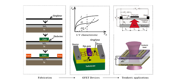
摘要: 石墨烯是单原子厚度的二维碳同素异形体材料,因其出色的电学、热学、光学及力学特性而被广泛应用于生物检测、医学、新能源、微电子、射频电路等领域。正是凭借着石墨烯独一无二的材料特性,石墨烯基场效应管(GFETs)比传统的硅基晶体管具有更高的迁移率、微缩空间及特征频率。此外,石墨烯零带隙的对称圆锥形能带结构,以及在受外部激发下形成的负电导率特性(太赫兹频段),使得GFETs能广泛应用于太赫兹功能器件中,也为实现太赫兹技术商业化提供了一种兼容当前半导体产业技术的低成本选择。针对硅基晶体管发展面临的尺度瓶颈,本文综述了GFETs器件的基本结构、射频/太赫兹领域的主要特性以及制备工艺,并举例说明了其在太赫兹技术领域的最新应用。Abstract: Graphene-based field effect transistors (GFETs) have a higher charge mobility and a higher cut-off frequency than traditional silicon-based transistors and are also smaller. The symmetrical conical band structure of the graphene channel with no band gap and negative dynamic conductivity of graphene with optical pumping in the terahertz (THz) band make them widely applicable in THz function devices, which are low cost and compatible with current semiconductor technology. In this paper, the scaling challenges for silicon-based transistors are discussed, and the basic structure, fabrication process and the main characteristics (C-V and I-V) in the THz/RF region for GFETs and graphene nanoribbon FETs are reviewed. Their novel uses in terahertz technology such as a terahertz electronic injection laser, a FET terahertz detector, a broadband FET terahertz modulator and an oscillator are summarized.
-
Geim A K, Novoselov K S. The rise of graphene[J]. Nature Materials, 2007, 6(3):183-191. Novoselov K S, Geim A K, Morozov S V, et al. Electric Field Effect in Atomically Thin Carbon Films[J]. Science, 2004, 306(5696):666-669. Li Y F, Liu Y Z, Zhang W K, et al. Green synthesis of reduced graphene oxide paper using Zn powder for supercapacitors[J]. Mater Lett, 2015, 157:273-276. Li Shao-juan, Gan Sheng, Mu Hao-ran, et al. Research progress in graphene use in photonic and optoelectronic devices[J]. New Carbon Materials, 2014, 29(5):329-356. Liu Y Z, Li Y F, Yuan S X, et al. Synthesis of 3D N, S dual-doped porous carbons with ultrahigh surface areas for highly efficient oxygen reduction reactions[J]. Chem Elctro Chem, 2018, 5:3506-3513. Singh V, Joung D, Zhai L, et al. Graphene based materials:Past, present and future[J]. Progress in Materials Science, 2011, 56(8):1178-1271. Robinson J a, Snyder D, Fanton M, et al. Development of graphene for high frequency electronics[C]. Electron Devices Meeting (IEDM). 2009 IEEE International, 2009:237-240. Jacob A P, Xie R, Sung M G, et al. Scaling challenges for advanced CMOS devices[J]. International Journal of High Speed Electronics and Systems, 2017, 26(01-02):1740001. Moore G E. No exponential is forever:But 'forever' can be delayed![C]. IEEE Internation Solid-State Circuits Conference. ISSCC, 2003, 2:1-19. Siers S, Damaraju S, George V, et al. The first 22nm IA multi-CPU and GPU system-on-chip using tri-gate transistors[C]. Solid State Circuits Conference (A-SSCC), 2012 IEEE Asian. IEEE, 2012:9-12. Bawankar M. Ⅲ-V Mosfet alternative TO Si/SiO2 mosfet[J]. Journal of Electronics & Communication Engineering, 2008:60-64. Lin J Q, Antoniadis D A, Del Alamo J A, et al. Novel intrinsic and extrinsic engineering for high-performance high-density self-aligned in GaAs Mosfets:Precise channel thickness control and sub-40-nm metal contacts[C]. Electron Devices Meeting (Iedm), 2014 IEEE International. IEEE, 2014:25.1.1-25.1.4. Lemme M C, Echtermeyer T J, Baus M, et al. A graphene field effect device[J]. Electronics, 2007, 28(4):1-12. Reddy D, Register L F, Carpenter G D, et al. Graphene field-effect transistors[J]. Journal of Physics D:Applied Physics, 2011, 44(31):313001. Schwierz F. Graphene transistors[J]. Nature Nanotechnology, 2010, 5(7):487-496. Hartmann R R, Kono J, Portnoi M E. Terahertz science and technology of carbon nanomaterials[J]. Nanotechnology, 2014, 25(32):32001. Lee M, Wanke M C. Searching for a solid-state terahertz technology[J]. Science, 2007, 316(5821):64-65. Lin Y-M, Dimitrakopoulos C, Jenkins K A, et al. 100 GHz transistors from wafer scale epitaxial graphene[J]. Science, 2010, 327(5699):662. Lin Y M, Valdes-Garcia A, Han S J, et al. Wafer-scale graphene integrated circuit[J]. Science, 2011, 332(6035):1294-1297. Vicarelli L, Vitiello M S, Coquillat D, et al. Graphene field-effect transistors as room-temperature terahertz detectors[J]. Nature Materials, 2012, 11(10):865-871. Petrone N, Meric I, Chari T, et al. Graphene field-effect transistors for radio-frequency flexible electronics[J]. IEEE Journal of the Electron Devices Society, 2015, 3(1):44-48. Dontschuk N, Stacey A, Tadich A, et al. A graphene field-effect transistor as a molecule-specific probe of DNA nucleobases[J]. Nature Communications, 2015, 6:1-7. Wang G, Zhang B, Ji H, et al. Monolayer graphene based organic optical terahertz modulator[J]. Applied Physics Letters, 2017, 110(2):23301. Novoselov K S, Geim A K, Morozov S V, et al. Room-temperature electric field effect and carrier-type inversion in graphene films[J]. ArXiv Preprint Cond-mat/0410631, 2004. Chen B, Liu H, Li X, et al. Fabrication of a graphene field effect transistor array on microchannels for ethanol sensing[J]. Applied Surface Science, 2012, 258(6):1971-1975. Zhang B Y, Liu T, Meng B, et al. Broadband high photoresponse from pure monolayer graphene photodetector[J]. Nature Communications, 2013, 4:1811. Zhan B, Li C, Yang J, et al. Graphene field-effect transistor and its application for electronic sensing[J]. Small, 2014, 10(20):4042-4065. Farmer D B, Chiu H Y, Lin Y M, et al. Utilization of a buffered dielectric to achieve high field-effect carrier mobility in graphene transistors[J]. Nano Letters, 2009, 9(12):4474-4478. Molitor F, Güttinger J, Stampfer C, et al. Local gating of a graphene Hall bar by graphene side gates[J]. Physical Review B, 2007, 76(24):245426. Tian J F, Jauregui L A, Lopez G, et al. Ambipolar graphene field effect transistors by local metal side gates[J]. Applied Physics Letters, 2010, 96(26):263110. Chen C, Low T, Chiu H, et al. Graphene side gate engineering[J]. IEEE Electron Device Letters, 2012, 33(3):330-332. Hähnlein B, Händel B, Pezoldt J, et al. Side-gate graphene field-effect transistors with high transconductance[J]. Applied Physics Letters, 2012, 101(9):93504. Zhang Q, Fang T, Xing H, et al. Graphene nanoribbon tunnel transistors[J]. IEEE Electron Device Letters, 2008, 29(12):1344-1346. Svintsov D, Vyurkov V V, Lukichev V F, et al. Tunnel field-effect transistors with graphene channels[J]. Semiconductors, 2013, 47(2):279-284. Malec C E, Davidovi D. Transport in graphene tunnel junctions[J]. Journal of Applied Physics, 2011, 109(6):064507(1-7). Britnell L, Gorbachev R V, Jalil R, et al. Field-effect tunneling transistor based on vertical graphene heterostructures[J]. Science, 2012, 335(6071):947-950. Schwierz F, Wong H, Liou J. Nanometer CMOS[M]. Pan Stanford Publishing, 2010. Wang H, Hsu A, Lee D S, et al. Delay analysis of graphene field-effect transistors[J]. IEEE Electron Device Letters, 2012, 33(3):324-326. Moon J S, Antcliffe M, Seo H C, et al. Graphene review:An emerging RF technology[C]. Silicon Monolithic Integrated Circuits in RF Systems (SiRF), 2012 IEEE 12th Topical Meeting on. IEEE, 2012:199-202. Schwierz F, Liou J. Modern microwave transistors:theory, design, and performance[M]. Wiley-Interscience, 2003. Schroder D K. Semiconductor Material and Device Characterization[M]. John Wiley & Sons, 2006. Nguyen L D, Tasker P J, Radulescu D C, et al. Design fabrication and characterization of ultra high speed AlGaAs/InGaAs MODFETs[C]. Electron Devices Meeting, 1988. IEDM'88. Technical Digest, International. IEEE, 1988:176-179. Hughes B, Tasker P J. Bias dependence of the MODFET intrinsic model elements values at microwave frequencies[J]. IEEE Transactions on Electron Devices, 1989, 36(10):2267-2273. Morozov S V, Novoselov K S, Katsnelson M I, et al. Giant intrinsic carrier mobilities in graphene and its bilayer[J]. Physical Review Letters, 2008, 100(1):4-8. Frank D J, Taur Y, Wong H P, et al. Generalized scale length for two-dimensional effects in Mosfets[J]. IEEE Electron Device Letters, 1998, 19(10):385-387. Meric I, Baklitskaya N, Kim P, et al. RF performance of top-gated, zero-bandgap graphene field-effect transistors[C]. Electron Devices Meeting, 2008. IEDM 2008. IEEE International. 2008:1-4. Liao L, Lin Y-C, Bao M, et al. High-speed graphene transistors with a self-aligned nanowire gate.[J]. Nature, 2010, 467(7313):305-308. Cheng R, Bai J, Liao L, et al. High-frequency self-aligned graphene transistors with transferred gate stacks[J]. Proceedings of the National Academy of Sciences, 2012, 109(29):11588-11592. Fang T, Konar A, Xing H, et al. Carrier statistics and quantum capacitance of graphene sheets and ribbons[J]. Applied Physics Letters, 2007, 91(9):92109. Zhong H, Zhang Z, Chen B, et al. Realization of low contact resistance close to theoretical limit in graphene transistors[J]. Nano Research, 2015, 8(5):1669-1679 Robinson J A, Labella M, Zhu M, et al. Contacting graphene[J]. Applied Physics Letters, 2011, 98(5):53203. Li W, Liang Y, Yu D, et al. Ultraviolet/ozone treatment to reduce metal-graphene contact resistance[J]. Applied Physics, 2013, 102(18):183110. Leong W S, Nai C T, Thong J T L. What does annealing do to metal-graphene contacts?[J]. Nano Letters, 2014, 14(7):3840-3847. Lemaitre M G, Donoghue E P, Mccarthy M a, et al. Improved transfer of graphene for organic, field-effect transistors[J]. ACS nano, 2012, 6(10):9095-9102. Gahoi A, Wagner S, Bablich A, et al. Contact resistance study of various metal electrodes with CVD graphene[J]. Solid-State Electronics, 2016, 125:234-239. Hong S K, Jeon S C, Hwang W S, et al. Resistance analysis and device design guideline for graphene RF transistors[J]. 2D Materials, 2015, 2(3):34011. Dean C R, Young A F, Meric I, et al. Boron nitride substrates for high-quality graphene electronics[J]. Nature Nanotechnology, 2010, 5(10):722-726. Wang H, Hsu A L, Palacios T. Graphene electronics for RF applications[J]. IEEE Microwave Magazine, 2012, 13(4):114-125. Hong S K, Oh J G, Hwang W S, et al. Enhanced performance in graphene RF transistors via advanced process integration[J]. Semiconductor Science and Technology, 2017, 32(4):45009. Franklin A D, Han S J, Bol A A, et al. Effects of nanoscale contacts to graphene[J]. IEEE Electron Device Letters, 2011, 32(8):1035-1037. Meric I, Dean C R, Young A. Graphene field-effect transistors based on boron nitride gate dielectrics[J]. Proceedings of the IEEE, 2013, 101(7):1609-1619. Nguyen V H, Bournel A, Chassat C. Quantum transport of Dirac fermions in graphene field effect transistors[C]. Simulation of Semiconductor Processes and Devices, 2010 International Conference on. IEEE, 2010:9-12. Falkovsky L A, Varlamov A A. Space-time dispersion of graphene conductivity[J]. European Physical Journal B, 2007, 56(4):281-284. Ando T, Zheng Y, Suzuura H. Dynamical conductivity and zero-mode anomaly in honeycomb lattices[J]. Journal of the Physical Society of Japan, 2002, 71(5):1318-1324. Sensale-rodriguez B, Member S, Yan R, et al. Graphene for reconfigurable THz optoelectronics[J]. Proceedings of the IEEE, 2013, 101(7):1705-1716. Matsumoto K. Frontiers of Graphene and Carbon Nanotubes[M]. Springer, 2015. Ferrari A C, Meyer J C, Scardaci V, et al. Raman spectrum of graphene and graphene layers[J]. Physical Review Letters, 2006, 97(18):187401. Kedzierski J, Hsu P-L, Healey P, et al. Epitaxial graphene transistors on SiC substrates[J]. IEEE Transactions on Electron Devices, 2008, 55(8):2078-2085. Kumar S, McEvoy N, Kim H Y, et al. CVD growth and processing of graphene for electronic applications[J]. Physica Status Solidi (B), 2011, 248(11):2604-2608. Wei W, Deokar G, Belhaj M, et al. Fabrication and characterization of CVD-grown graphene based Field-Effect Transistor[C]. EMicrowave Conference (EuMC), 201444th European. IEEE, 2014:367-370. Regan W, Alem N, Alemán B, et al. A direct transfer of layer-area graphene[J]. Applied Physics Letters, 2010, 96(11):113102. Lee B, Park S-Y, Kim H-C, et al. Conformal Al2O3 dielectric layer deposited by atomic layer deposition for graphene-based nanoelectronics[J]. Applied Physics Letters, 2008, 92(20):203102. Kim S, Nah J, Jo I, et al. Realization of a high mobility dual-gated graphene field effect transistor with Al2O3 dielectric[J]. 2009, 94(6):62107. Novoselov K S, Geim A K, Morozov S V, et al. Two-dimensional gas of massless Dirac fermions in graphene[J]. Nature, Nature Publishing Group, 2005, 438(7065):197-200. Castro Neto A H, Guinea F, Peres N M R, et al. The electronic properties of graphene[J]. Reviews of Modern Physics, 2009, 81(1):109-162. Ryzhii V, Ryzhii M, Satou A, et al. Graphene-based terahertz devices:Concepts and characteristics[J]. Future Trends in Microelectronics:From Nanophotonics to Sensors and Energy, 2010:293-306. Ryzhii V, Ryzhii M, Otsuji T. Negative dynamic conductivity of graphene with optical pumping[J]. Journal of Applied Physics, 2007, 101(8):83114. Breusing M, Ropers C, Elsaesser T. Ultrafast carrier dynamics in graphite[J]. Physical Review Letters, 2009, 102(8):86809. George P A, Strait J, Dawlaty J, et al. Ultrafast optical-pump terahertz-probe spectroscopy of the carrier relaxation and recombination dynamics in epitaxial graphene[J]. Nano Letters, 2008, 8(12):4248-4251. Dawlaty J M, Shivaraman S, Chandrashekhar M, et al. Measurement of ultrafast carrier dynamics in epitaxial graphene[J]. Applied Physics Letters, 2008, 92(4):42116. Satou A, Ryzhii V, Kurita Y, et al. Threshold of terahertz population inversion and negative dynamic conductivity in graphene under pulse photoexcitation[J]. Journal of Applied Physics, 2013, 113(14):143108. Satou A, Otsuji T, Ryzhii V. Theoretical study of population inversion in graphene under pulse excitation[J]. Japanese Journal of Applied Physics, 2011, 50(7):70116. Dubinov A A, Aleshkin V Y, Ryzhii M, et al. Terahertz laser with optically pumped graphene layers and fabri-perot resonator[J]. Applied Physics Express, 2009, 2(9):92301. Ryzhii V, Ryzhii M, Satou A, et al. Feasibility of terahertz lasing in optically pumped epitaxial multiple graphene layer structures[J]. Journal of Applied Physics, 2009, 106(8):84507. Ryzhii V, Dubinov A A, Otsuji T, et al. Terahertz lasers based on optically pumped multiple graphene structures with slot-line and dielectric waveguides[J]. Journal of Applied Physics, 2010, 107(5):54505. Ryzhii V, Ryzhii M, Mitin V, et al. Toward the creation of terahertz graphene injection laser[J]. Journal of Applied Physics, 2011, 110(9):94503. Tamamushi G, Watanabe T, Mitsushio J, et al. Current-injection terahertz lasing in a distributed-feedback dual-gate graphene-channel transistor[C]. Proc of SPIE, 2017, 10111:1011126. Popov V V, Polischuk O V, Davoyan A R, et al. Plasmonic terahertz lasing in an array of graphene nanocavities[J]. Physical Review B, 2012, 86(19):195437. Otsuji T, Watanabe T. Graphene active plasmonic metamaterials for new types of terahertz lasers[C]. SPIE Defense, Security, and Sensing. International Society for Optics and Photonics, 2013:87160P1-12. Lü J Q, Shur M S, Hesler J L, et al. Terahertz detector utilizing two-dimensional electronic fluid[J]. IEEE Electron Device Letters, 1998, 19(10):373-375. He X, Fujimura N, Lloyd J M, et al. Carbon nanotube terahertz detector[J]. Nano Letters, 2014, 14(7):3953-3958. Marczewski J, Knap W, Tomaszewski D, et al. Silicon junctionless field effect transistors as room temperature terahertz detectors[J]. Journal of Applied Physics, 2015, 118(10):104502. Nair R R, Blake P, Grigorenko N, et al. Fine structure constant defines visual transperency of graphene[J]. Science, 2008, 320(5881):1308. Wang F, Zhang Y, Tian C, et al. Gate-variable optical transitions in graphene[J]. Science, 2008, 320(5873):206-209. Xia F, Mueller T, Lin Y, et al. Ultrafast graphene photodetector[J]. Nature Nanotechnology, 2009, 4(12):839-843. Ryzhii V, Ryzhii M. Graphene bilayer field-effect phototransistor for terahertz and infrared detection[J]. Physical Review B, 2009, 79(24):245311. Ryzhii V, Ryzhii M, Mitin V, et al. Terahertz and infrared photodetection using p-i-n multiple-graphene-layer structures[J]. Journal of Applied Physics, 2010, 107(5):54512. Zak A, Andersson M A, Bauer M, et al. Antenna-integrated 0.6 THz FET direct detectors based on CVD graphene[J]. Nano Letters, 2014, 14(10):5834-5838. Dyakonov M, Shur M. Plasma ectronics:Nove rahertz devices using[J]. IEEE Transactions on Electron Devices, 1996, 43(10):1640-1645. Svintsov D, Leiman V G, Ryzhii V, et al. Graphene nanoelectro mechanical resonators for the detection of modulated terahertz radiation[J]. Journal of Physics D:Applied Physics, 2014, 47(50):505105. Ryzhii V, Otsuji T, Ryzhii M, et al. Resonant plasmonic terahertz detection in vertical graphene-base hot-electron transistors[J]. Journal of Applied Physics, 2015, 118(20):204501. Dhillon S S, Vitiello M S, Linfield E H, et al. The 2017 terahertz science and technology roadmap[J]. Journal of Physics D:Applied Physics, 2017, 50(4):43001. Lee S H, Choi M, Kim T T, et al. Gate-controlled active graphene metamaterials at terahertz frequencies[J]. Technical Digest - 201217th Opto-Electronics and Communications Conference, OECC 2012, 2012, 11(11):582-583. Chen H-T, Padilla W J, Zide J M O, et al. Active terahertz metamaterial devices[J]. Nature, 2006, 444(7119):597-600. Paul O, Imhof C, Lägel B, et al. Polarization-independent active metamaterial for high-frequency terahertz modulation[J]. Optics express, 2009, 17(2):819-827. Rouhi N, Capdevila S, Jain D, et al. Terahertz graphene optics[J]. Nano Research, 2012, 5(10):667-678. Tassin A P, Koschny T, Soukoulis C M. Graphene for Terahertz Applications[J]. Science, 2013, 341(6146):620-621. Sensale-Rodriguez B, Fang T, Yan R, et al. Unique prospects for graphene-based terahertz modulators[J]. Applied Physics Letters, 2011, 99(11):113104. Sensale-Rodriguez B, Yan R, Kelly M M, et al. Broadband graphene terahertz modulators enabled by intraband transitions.[J]. Nature communications, 2012, 3:780. Dawlaty J M, Shivaraman S, Strait J, et al. Measurement of the optical absorption spectra of epitaxial graphene from terahertz to visible[J]. Applied Physics Letters, 2008, 93(13):131905. Choi H, Borondics F, Siegel D A, et al. Broadband electromagnetic response and ultrafast dynamics of few-layer epitaxial graphene[J]. Applied Physics Letters, 2009, 94(17):172102. Ryzhii V, Otsuji T, Ryzhii M, et al. Effect of plasma resonances on dynamic characteristics of double graphene-layer optical modulator[J]. Journal of Applied Physics, 2012, 112(10):104507. Liang G, Hu X, Yu X, et al. Integrated terahertz graphene modulator with 100% modulation depth[J]. ACS Photonics, 2015, 2(11):1559-1566. Rana F. Graphene Terahertz Plasmon Oscillators[J]. IEEE Transactions on Nanotechnology, 2008, 7(1):91-99. Takatsuka Y, Sano E, Ryzhii V, et al. Terahertz amplifiers based on multiple graphene layer with field-enhancement effect[J]. Japanese Journal of Applied Physics, 2011, 50(7):70118. Azar O A, Abdi M, Baghban H. Graphene-based terahertz waveguide amplifier[J]. Procedia Materials Science, 2015, 11:270-274. Mao X, Cheng C, Huang B, et al. Optoelectronic mixer based on graphene FET[J]. IEEE Electron Device Letters, 2015, 36(3):253-255. Chen P Y, Argyropoulos C, Alu A. Terahertz antenna phase shifters using integrally-gated graphene transmission-lines[J]. IEEE Transactions on Antennas and Propagation, 2013, 61(4):1528-1537. -

 下载:
下载:
 点击查看大图

图(1)
计量
- 文章访问数: 691
- HTML全文浏览量: 279
- PDF下载量: 497
- 被引次数: 0