Preparation of nano-diamond films on GaN with a Si buffer layer
-
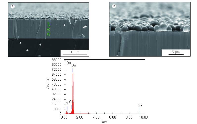
摘要: 本文研发了一种简便有效的在GaN半导体衬底上直接生长纳米金刚石膜的方法。研究发现,直接将GaN衬底暴露于氢等离子体中5 min即发生分解,且随着温度从560℃升高至680℃,这种分解反应愈加剧烈,很难在GaN衬底上直接形成结合力良好的纳米金刚石膜。通过在GaN衬底上镀制几纳米厚的硅过渡层,在富氢金刚石生长环境下,抑制了GaN衬底的分解,同时在GaN衬底上沉积了约2 μm厚的纳米金刚石膜。硅过渡层厚度是决定纳米金刚石与GaN衬底结合力的主要因素。当硅过渡层厚度为10 nm时,纳米金刚石膜与GaN衬底呈现出大于10 N的结合力,可能与硅过渡层在金刚石生长过程中向SiC过渡层转变有关。Abstract: Gallium nitride (GaN) has been widely used in electronic and optoelectronic devices because of its unique electrical properties. However, its low thermal conductivity and the high thermal boundary resistance at the interface between GaN and substrates such as Si and Al2O3 prevent efficient heat dissipation from the heated regions, which limits the further development of GaN-based high power devices. Diamond, with the highest thermal conductivity, has been considered to be one of the most promising heat sink materials. However, it is hard to prepare a diamond film on a GaN substrate because there is a high thermal expansion coefficient difference and also a large lattice mismatch between them. An approach to prepare a nano-diamond film on a GaN substrate by incorporating a Si buffer layer has been proposed. A GaN substrate decomposes significantly from 560 to 680℃ when exposed to ahydrogen plasma for 5 min and no adhesive nano-diamond film can be directly grown on it. This decomposition is significantly suppressed by the presence of a Si buffer layer and a nano-diamond film about 2 μm thick can be deposited on a GaN substrate by microwave chemical vapor deposition using CH4 as the carbon source. With an optimum Si layer of 10 nm, the adhesive force between the nano-diamond film and the GaN substrate reaches 10N, which is ascribed to the complete conversion of the Si layer to a silicon carbidetransition layer during the deposition.
-
Key words:
- GaN /
- Si buffer layer /
- Nano-diamond film /
- Direct growth /
- Decomposition
-
Gelmont B, Kim K, Shur M. Monte carlo simulation of electron transport in gallium nitride[J]. Journal of Applied Physics, 1993, 74(3): 1818-1821. Zhang D, Bian J M, Qin F W, et al. Highly c-axis oriented GaN films grown on free-standing diamond substrates for high-power devices[J]. Materials Research Bulletin, 2011, 46(10): 1582-1585. Gaska R, Yang J W, Osinsky A, et al. Electron transport in AlGaN heterostructures grown on 6H-SiC substrates[J]. Applied Physics Letters, 1998, 72(6): 707-709. Sadi T, Kelsal R W, Pilgrim N J. Investigation of self-heating effects in submicrometer GaN/AlGaN HEMTs using an electrothermal Monte Carlo method[J]. IEEE Transactions on Electron Devices, 2006, 53(12): 2892-2900. Trew R J, Green D S, Shealy J B. AlGaN/GaN HFET reliability[J]. IEEE Microwave Magazine, 2009, 10(4): 116-127. Kuball M, Hayes J M, Uren M J, et al. Measurement of temperature in active high-power AlGaN/GaN HFETs using Raman spectroscopy[J]. IEEE Eletron Device Letters, 2002, 23(1): 7-9. Felbinger J G, Chandra M V S, Sun Y J, et al. Comparison of GaN HEMTs on diamond and SiC substrates[J]. IEEE Eletron Device Letters, 2007, 28(11): 948-950. Wu Y F, Saxler A, Moore M, et al. 30W/mm GaN HEMTs by field plate optimization[J]. IEEE Electron Device Letters, 2004, 25(3): 117-119. Govindaraju N, Singh R N. Processing of nanocrystalline diamond thin films for thermal manage-ment of wide-bandgap semiconductor power electronics[J]. Materials Science and Engineering: B, 2011, 176(14): 1058-1072. Diduck Q, Felbinger J, Eastman L F, et al. Frequency performance enhancement of AlGaN/GaN HEMTs on diamond[J]. Electron Letters, 2009, 45(14): 758-759. Goyal V, Sumant A V, Teweldebrhan D, et al. Direct low-temperature integration of nano-crystalline diamond with GaN substrates for improved thermal management of high-power electronics[J]. Advanced Functional Materials, 2012, 22(7): 1525-1530. Joshi B C, Dhanavantri C, Kumar D. Sapphire, SiC, AlN, Si and diamond-substrate material for GaN HEMT and LED[J]. Journal of Optoelectronics and Advanced Materials, 2009, 11(8): 1111-1116. Zhang D, Bai Y Z, Qin F W, et al. Preparation and characteristics of GaN films on freestanding CVD thick diamond films[J]. Chinese Physics Letters, 2010, 27(1): 018102-018102-4. Zimmer J W, Chandler G. Advances in large diameter GaN on diamond substrates [C]. CS Mantech Conference, Chicago, USA, April 14-17, 2008. Zou Y S, Yang Y, Chong Y M, et al. Chemical vapor deposition of diamond films on patterned GaN substrates via a thin silicon nitride protective layer[J]. Crystal Growth and Design, 2008, 8(5): 1770-1773. May P W, Tsai H Y, Wang W N, et al. Deposition of CVD diamond onto GaN[J]. Diamond and Related Materials, 2006, 15(4-8): 526-530. Francis D, Faili F, Babi D, et al. Formation and characterization of 4-inch GaN-on-diamond substrates[J]. Diamond and Related Materials, 2010, 19(2-3): 229-233. Hageman P R, Schermer J J, Larsen P K. GaN growth on single-crystal diamond substrate by metalorganic chemical vapour deposition and hydride vapour deposition[J]. Thin Solid Film, 2003, 443(1-2): 9-13. Yeh Y H, Chen K M, Wu Y H, et al. Hydrogen etching of GaN and its application to produce free-standing GaN thick films[J]. Journal of Crystal Growth, 2011, 333(1): 16-19. Alomari M, Dipalo M, Rossi S, et al. Diamond overgrown InAlN/GaN HEMT [J]. Diamond and Related Materials, 2011, 20(4): 604-608. -

 下载:
下载:
 点击查看大图

图(1)
计量
- 文章访问数: 439
- HTML全文浏览量: 110
- PDF下载量: 539
- 被引次数: 0