Graphene-based in-plane heterostructures for atomically thin electronics
-
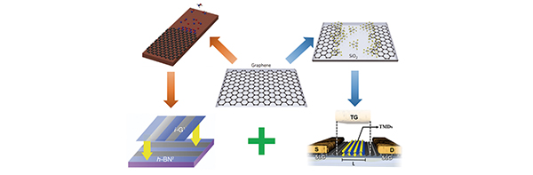
摘要: 二维平面晶体,由于能带结构的多样性和与半导体平面工艺兼容的特点,被认为在电子学中是延续摩尔定律的候选材料之一;同时它具备易转移、光学透明、能带可调等特点,在柔性电子学和光电子学方面展示出巨大的潜在应用。将电路所需的具有不同导电性能的二维材料在平面内实现空间上的可控集成,是实现单原子层二维电子学的首要问题。综述了最近在石墨烯基电子学中平面异质结的研究进展,包括石墨烯-绝缘体和石墨烯-半导体异质结,集中在可控制备、对界面结构的原子尺度研究、以及逻辑功能原型器件研究。最后简述当前该领域面临的挑战和研究前景。Abstract: Two-dimensional materials are promising for use in atomically thin electronics, optoelectronics and flexible electronics because of their versatile band structures, optical transparency, easy transfer to a substrate and compatibility with current technology for integrated circuits. Three key components of contemporary integrated circuits, metals, insulators and semiconductors, have analogues in two-dimensional materials, i.e., graphene, boron nitride (BN) and transition metal dichalcogenides (TMDCs), respectively. Their controlled integration in a single layer is essential for achieving completely two-dimensional devices. In this review, we briefly describe the latest advances in graphene-based planar heterostructures, in graphene-BN, and in graphene-TMDC heterojunctions, focusing on the fabrication methods, the interfacial structure characteristics at the atomic scale and the properties of prototype electronic devices. The challenges and prospects in this field are also discussed.
-
Key words:
- Graphene /
- In-plane heterostructure /
- Interface structure /
- Field-effect transistor /
- Logic device
-
Moore G E. Cramming more components onto integrated circuits, Reprinted from Electronics, volume 38, number 8, April 19, 1965, pp. 114 ff[J]. IEEE Solid-State Circuits Society Newsletter, 2006, 11(3):33-35. Novoselov K S, Geim A K, Morozov S V, et al. Electric field effect in atomically thin carbon films[J]. Science, 2004, 306(5696):666-669. Geim A K, Novoselov K S. The rise of graphene[J]. Nature Materials, 2007, 6(3):183-191. Geim A K. Graphene:Status and prospects[J]. Science, 2009, 324(5934):1530-1534. Morozov S V, Novoselov K S, Katsnelson M I, et al. Giant intrinsic carrier mobilities in graphene and its bilayer[J]. Physical Review Letters, 2008, 100(1):016602. Mayorov A S, Gorbachev R V, Morozov S V, et al. Micrometer-scale ballistic transport in encapsulated graphene at room temperature[J]. Nano Letters, 2011, 11(6):2396-2399. Loh K P, Bao Q, Ang P K, et al. The chemistry of graphene[J]. Journal of Materials Chemistry, 2010, 20(12):2277-2289. Guo J J, Mao Z, Yan X L, et al. Ultrasmall tungsten carbide catalysts stabilized in graphitic layers for high-performance oxygen reduction reaction[J]. Nano Energy, 2016, 28:261-268. Choi W, Lahiri I, Seelaboyina R, et al. Synthesis of graphene and its applications:a review[J]. Critical Reviews in Solid State and Materials Sciences, 2010, 35(1):52-71. Eda G, Fanchini G, Chhowalla M. Large-area ultrathin films of reduced graphene oxide as a transparent and flexible electronic material[J]. Nature Nanotechnology, 2008, 3(5):270-274. Akinwande D, Petrone N, Hone J. Two-dimensional flexible nanoelectronics[J]. Nature Communications, 2014, 5:5678-5689. Levendorf M P, Kim C J, Brown L, et al. Graphene and boron nitride lateral heterostructures for atomically thin circuitry[J]. Nature, 2012, 488(7413):627-632. Jo G, Choe M, Lee S, et al. The application of graphene as electrodes in electrical and optical devices[J]. Nanotechnology, 2012, 23(11):112001. Watanabe K, Taniguchi T, Kanda H. Direct-bandgap properties and evidence for ultraviolet lasing of hexagonal boron nitride single crystal[J]. Nature Materials, 2004, 3(6):404-409. Wang Q H, Kalantar-Zadeh K, Kis A, et al. Electronics and optoelectronics of two-dimensional transition metal dichalcogenides[J]. Nature Nanotechnology, 2012, 7(11):699-712. Zhang T, Fu L. Controllable chemical vapor deposition growth of two-dimensional heterostructures[J]. Chem, 2018, 4(4):671-689. Roy T, Liu L, De La Barrera S, et al. Tunneling characteristics in chemical vapor deposited graphene-hexagonal boron nitride-graphene junctions[J]. Applied Physics Letters, 2014, 104(12):123506. Meyyappan M, Delzeit L, Cassell A, et al. Carbon nanotube growth by PECVD:A review[J]. Plasma Sources Science and Technology, 2003, 12(2):205-216. Fu W Y, Liu L, Wang W L, et al. Carbon nanotube transistors with graphene oxide films as gate dielectrics[J]. Science China Physics, Mechanics and Astronomy, 2010, 53(5):828-833. Fortuna S A, Li X. Metal-catalyzed semiconductor nanowires:a review on the control of growth directions[J]. Semiconductor Science and Technology, 2010, 25(2):024005. Mattevi C, Kim H, Chhowalla M. A review of chemical vapour deposition of graphene on copper[J]. Journal of Materials Chemistry, 2011, 21(10):3324-3334. Li X, Cai W, An J, et al. Large-area synthesis of high-quality and uniform graphene films on copper foils[J]. Science, 2009, 324(5932):1312-1314. Reina A, Jia X, Ho J, et al. Large area, few-layer graphene films on arbitrary substrates by chemical vapor deposition[J]. Nano Letters, 2008, 9(1):30-35. Shi Y, Hamsen C, Jia X, et al. Synthesis of few-layer hexagonal boron nitride thin film by chemical vapor deposition[J]. Nano Letters, 2010, 10(10):4134-4139. Song L, Ci L, Lu H, et al. Large scale growth and characterization of atomic hexagonal boron nitride layers[J]. Nano Letters, 2010, 10(8):3209-3215. Ci L, Song L, Jin C, et al. Atomic layers of hybridized boron nitride and graphene domains[J]. Nature Materials, 2010, 9(5):430-435. Wang H, Zhao C, Liu L, et al. Towards the controlled CVD growth of graphitic B-C-N atomic layer films:the key role of B-C delivery molecular precursor[J]. Nano Research, 2016, 9(5):1221-1235. Huang P Y, Ruiz-Vargas C S, van der Zande A M, et al. Grains and grain boundaries in single-layer graphene atomic patchwork quilts[J]. Nature, 2011, 469(7330):389-392. Liu Z, Ma L, Shi G, et al. In-plane heterostructures of graphene and hexagonal boron nitride with controlled domain sizes[J]. Nature Nanotechnology, 2013, 8(2):119-124. Kim G, Lim H, Ma K Y, et al. Catalytic conversion of hexagonal boron nitride to graphene for in-plane heterostructures[J]. Nano Letters, 2015, 15(7):4769-4775. Liu L, Park J, Siegel D A, et al. Heteroepitaxial growth of two-dimensional hexagonal boron nitride templated by graphene edges[J]. Science, 2014, 343(6167):163-167. Vlassiouk I, Regmi M, Fulvio P, et al. Role of hydrogen in chemical vapor deposition growth of large single-crystal graphene[J]. ACS Nano, 2011, 5(7):6069-6076. Liu L, Siegel D A, Chen W, et al. Unusual role of epilayer-substrate interactions in determining orientational relations in van der Waals epitaxy[J]. Proceedings of the National Academy of Sciences, 2014, 111(47):16670-16675. Gao T, Song X, Du H, et al. Temperature-triggered chemical switching growth of in-plane and vertically stacked graphene-boron nitride heterostructures[J]. Nature Communications, 2015, 6:6835-6834. Zhang D, Zhang D B, Yang F, et al. Interface engineering of electronic properties of graphene/boron nitride lateral heterostructures[J]. 2D Materials, 2015, 2(4):041001. Zeng J, Chen W, Cui P, et al. Enhanced half-metallicity in orientationally misaligned graphene/hexagonal boron nitride lateral heterojunctions[J]. Physical Review B, 2016, 94(23):235425. Ramasubramaniam A, Naveh D. Carrier-induced antiferromagnet of graphene islands embedded in hexagonal boron nitride[J]. Physical Review B, 2011, 84(7):075405. Jiang J W, Wang J S, Wang B S. Minimum thermal conductance in graphene and boron nitride superlattice[J]. Applied Physics Letters, 2011, 99(4):043109. Guo J J, Lee J, Contescu C I, et al. Crown ethers in graphene[J]. Nature Communications, 2014, 5:5389-5395. Zhang X F, Guo J J, Guan P F, et al. Catalytically active single-atom niobium in graphitic layers[J]. Nature Communications, 2013, 4:1924-1930. Xu Z, Bando Y, Liu L, et al. Electrical conductivity, chemistry, and bonding alternations under graphene oxide to graphene transition as revealed by in situ TEM[J]. ACS Nano, 2011, 5(6):4401-4406. Han G H, Rodríguez-Manzo J A, Lee C W, et al. Continuous growth of hexagonal graphene and boron nitride in-plane heterostructures by atmospheric pressure chemical vapor deposition[J]. ACS Nano, 2013, 7(11):10129-10138. Lu J, Zhang K, Liu X F, et al. Order-disorder transition in a two-dimensional boron-carbon-nitride alloy[J]. Nature Communications, 2013, 4:2681-2687. Sutter P, Cortes R, Lahiri J, et al. Interface formation in monolayer graphene-boron nitride heterostructures[J]. Nano Letters, 2012, 12(9):4869-4874. Zhang X, Stradi D, Liu L, et al. Tunneling spectra of graphene on copper unraveled[J]. Physical Chemistry Chemical Physics, 2016, 18(25):17081-17090. Ma C, Park J, Liu L, et al. Interplay between intercalated oxygen superstructures and monolayer h-BN on Cu (100)[J]. Physical Review B, 2016, 94(6):064106. Gao Y, Zhang Y, Chen P, et al. Toward single-layer uniform hexagonal boron nitride-graphene patchworks with zigzag linking edges[J]. Nano Letters, 2013, 13(7):3439-3443. Mohsin A, Cross N G, Liu L, et al. Experimentally determined edge orientation of triangular crystals of hexagonal boron nitride[J]. Physica Status Solidi (b), 2017, 254(9):1700069. Liu M, Li Y, Chen P, et al. Quasi-freestanding monolayer heterostructure of graphene and hexagonal boron nitride on Ir (111) with a zigzag boundary[J]. Nano Letters, 2014, 14(11):6342-6347. Zhao R, Wang J, Yang M, et al. BN-embedded graphene with a ubiquitous gap opening[J]. The Journal of Physical Chemistry C, 2012, 116(39):21098-21103. Liu Y, Bhowmick S, Yakobson B I. BN white graphene with "colorful" edges:The energies and morphology[J]. Nano Letters, 2011, 11(8):3113-3116 Geim A K, Grigorieva I V. Van der Waals heterostructures[J]. Nature, 2013, 499(7459):419-425. Park J, Lee J, Liu L, et al. Spatially resolved one-dimensional boundary states in graphene-hexagonal boron nitride planar heterostructures[J]. Nature Communications, 2014, 5:5403-5408. Li Y, Mazzarello R. Structural and electronic properties of hybrid graphene and boron nitride nanostructures on Cu[J]. Physical Review B, 2013, 88(4):045317. Rui Dong, and Irma Kuljanishvili. Progress in fabrication of transition metal dichalcogenides heterostructure systems[J]. Journal of Vacuum Science & Technology B. 35, 030803(2017). Hermes S, Schröter M K, Schmid R, et al. Metal@MOF:loading of highly porous coordination polymers host lattices by metal organic chemical vapor deposition[J]. Angewandte Chemie International Edition, 2005, 44(38):6237-6241. Yan S, Maeda H, Kusakabe K, et al. Thin palladium membrane formed in support pores by metal-organic chemical vapor deposition method and application to hydrogen separation[J]. Industrial & Engineering Chemistry Research, 1994, 33(3):616-622. Park D, Kim Y H, Lee J K. Synthesis of carbon nanotubes on metallic substrates by a sequential combination of PECVD and thermal CVD[J]. Carbon, 2003, 41(5):1025-1029. Zhao M, Ye Y, Han Y, et al. Large-scale chemical assembly of atomically thin transistors and circuits[J]. Nature Nanotechnology, 2016, 11(11):954-959. Tang H L, Chiu M H, Tseng C C, et al. Multilayer Graphene-WSe2 Heterostructures for WSe2 Transistors[J]. ACS Nano, 2017, 11(12):12817-12823. Grieg D D, Engelmann H F. Microstrip-A new transmission technique for the klilomegacycle range[J]. Proceedings of the IRE, 1952, 40(12):1644-1650. Cho C S, Lee J W, Kim J. Dual-and triple-mode branch-line ring resonators and harmonic suppressed half-ring resonators[J]. IEEE Transactions on Microwave Theory and Techniques, 2006, 54(11):3968-3974. Allain A, Kang J, Banerjee K, et al. Electrical contacts to two-dimensional semiconductors[J]. Nature Materials, 2015, 14(12):1195-1205. Kappera R, Voiry D, Yalcin S E, et al. Phase-engineered low-resistance contacts for ultrathin MoS2 transistors[J]. Nature Materials, 2014, 13(12):1128-1134. Yu L, Lee Y H, Ling X, et al. Graphene/MoS2 hybrid technology for large-scale two-dimensional electronics[J]. Nano Letters, 2014, 14(6):3055-3063. Cheng R, Jiang S, Chen Y, et al. Few-layer molybdenum disulfide transistors and circuits for high-speed flexible electronics[J]. Nature Communications, 2014, 5:5143-5151. Duan X, Wang C, Shaw J C, et al. Lateral epitaxial growth of two-dimensional layered semiconductor heterojunctions[J]. Nature Nanotechnology. 2014, 9:1024-1030. Tosun M, Chuang S, Fang H, et al. High-gain inverters based on WSe2 complementary field-effect transistors[J]. ACS Nano, 2014, 8(5):4948-4953. Kim Y, Cruz S S, Lee K, et al. Remote epitaxy through graphene enables two-dimensional material-based layer transfer[J]. Nature, 2017, 544:340-343. Sarkar D, Xie X, Liu W, et al. A subthermionic tunnel field-effect transistor with an atomically thin channel[J]. Nature, 2017, 526:91-95. Tran T T, Wang D, Xu Z Q, et al. Deterministic coupling of quantum emitters in 2D materials to plasmonic nanocavity arrays[J]. Nano Letters, 2017, 17(4):2634-2639. -

 下载:
下载:
 点击查看大图

图(1)
计量
- 文章访问数: 402
- HTML全文浏览量: 67
- PDF下载量: 259
- 被引次数: 0