Flexible and lightweight graphene grown by rapid thermal processing chemical vapor deposition for thermal management in consumer electronics
-
摘要: 下一代电子产品的飞速发展对热管理提出了更高的要求。初始石墨烯的导热性是铜的13倍。本文通过快速热处理化学气相沉积(RTP-CVD)法制备了具有大sp2结构域的单层、双层和多层石墨烯(SLG、BLG、FLG),进一步通过低浓度H2还原制备了高导热石墨烯。在1 000 °C下生长25 min制备出SLG,利用拉曼光谱和透射电子显微镜(TEM)研究了石墨烯的品质。为了验证RTP-CVD法生成的石墨烯的散热能力,将其作为2TB固态硬盘的散热器,通过红外热成像仪进行了研究。结果证明,RTP-CVD生长的石墨烯用于消费电子产品的热管理测试时性能表现优异。SLG显示温度(最高)比商用铜散热器低5 °C,SLG的散热能力比商用铜散热器快200倍左右。综上,利用RTP-CVD法制备的轻质的柔性石墨烯可以成为下一代5G设备和消费电子产品热管理的更好选择。Abstract: Next-generation consumer electronics require excellent thermal management. Graphene is a good choice because its thermal conductivity is 13 times that of copper. Single-, bi- and few-layer graphene (SLG, BLG, FLG) with large sp2 domains were grown by rapid thermal processing chemical vapor deposition (RTP-CVD) from CH4 and H2 using Ar as the diluting gas. The quality of graphene was investigated by Raman spectroscopy and TEM. To demonstrate the heat dissipation capability of RTP-CVD-grown graphene, a 2 TB solid state drive was used and the temperature was measured by a FLIR thermal camera. Results indicate that high thermal conductivity graphene was prepared by diluting the precursor gas with Ar. SLG was prepared at a growth temperature of 1 000 °C and a time of 25 min. A transition from FLG to high-quality BLG was observed at low H2 concentrations. Using SLG, there was a 5 °C lower temperature rise than using a commercial copper heat dissipator. The heat dissipation ability of SLG was approximately 200 times that of commercial copper heat dissipators.
-
Key words:
- Graphene /
- Thermal management /
- Consumer electronics /
- Chemical vapour deposition
-

Figure 2. (a) The schematic representation of chemisorption/deposition of graphene on copper foil. Stage-I: dissociative dehydrogenation of CH4, Stage-II: dimerization, Stage-III & Stage-IV: trimerization and migration, and Stage-V: growth of graphene. FE-SEM images of (b) Ar-70, (c) Ar-80 and (d) Ar-100 samples

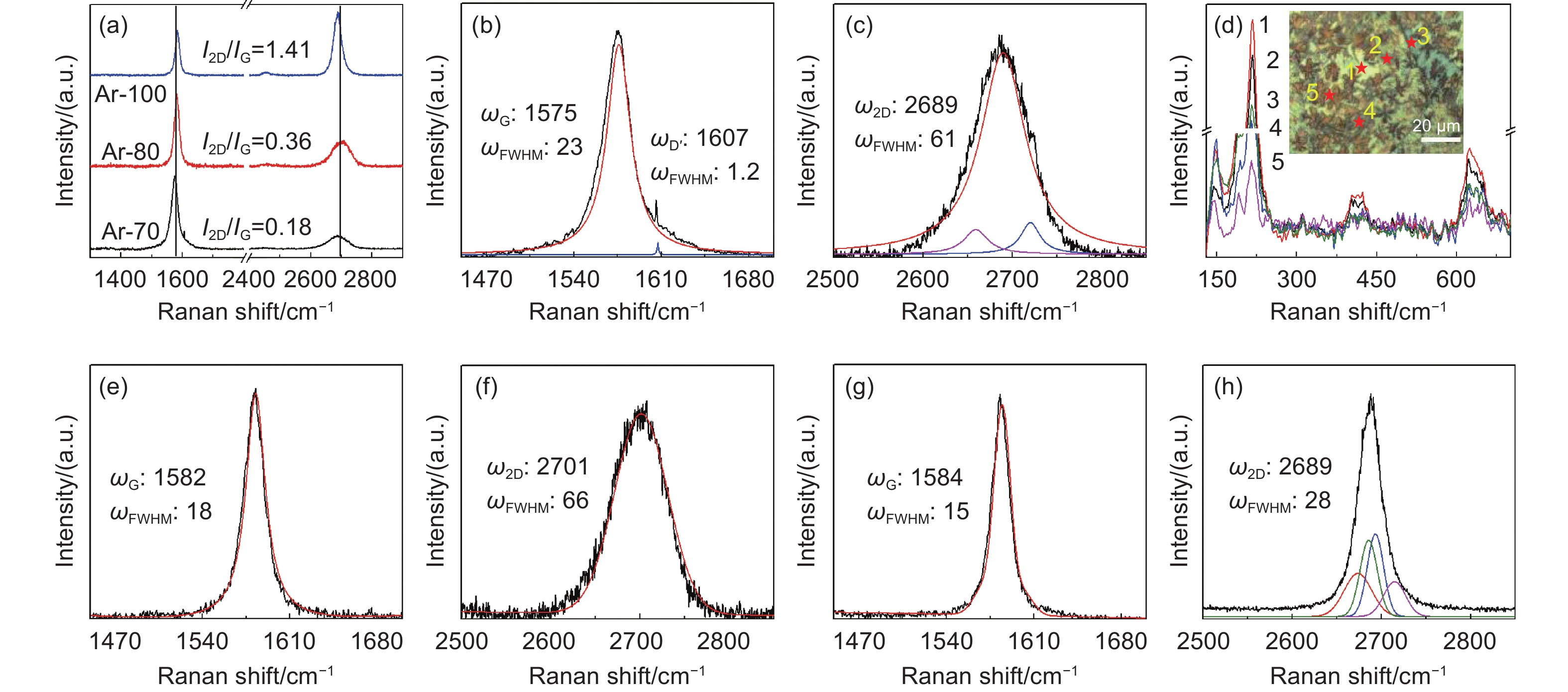
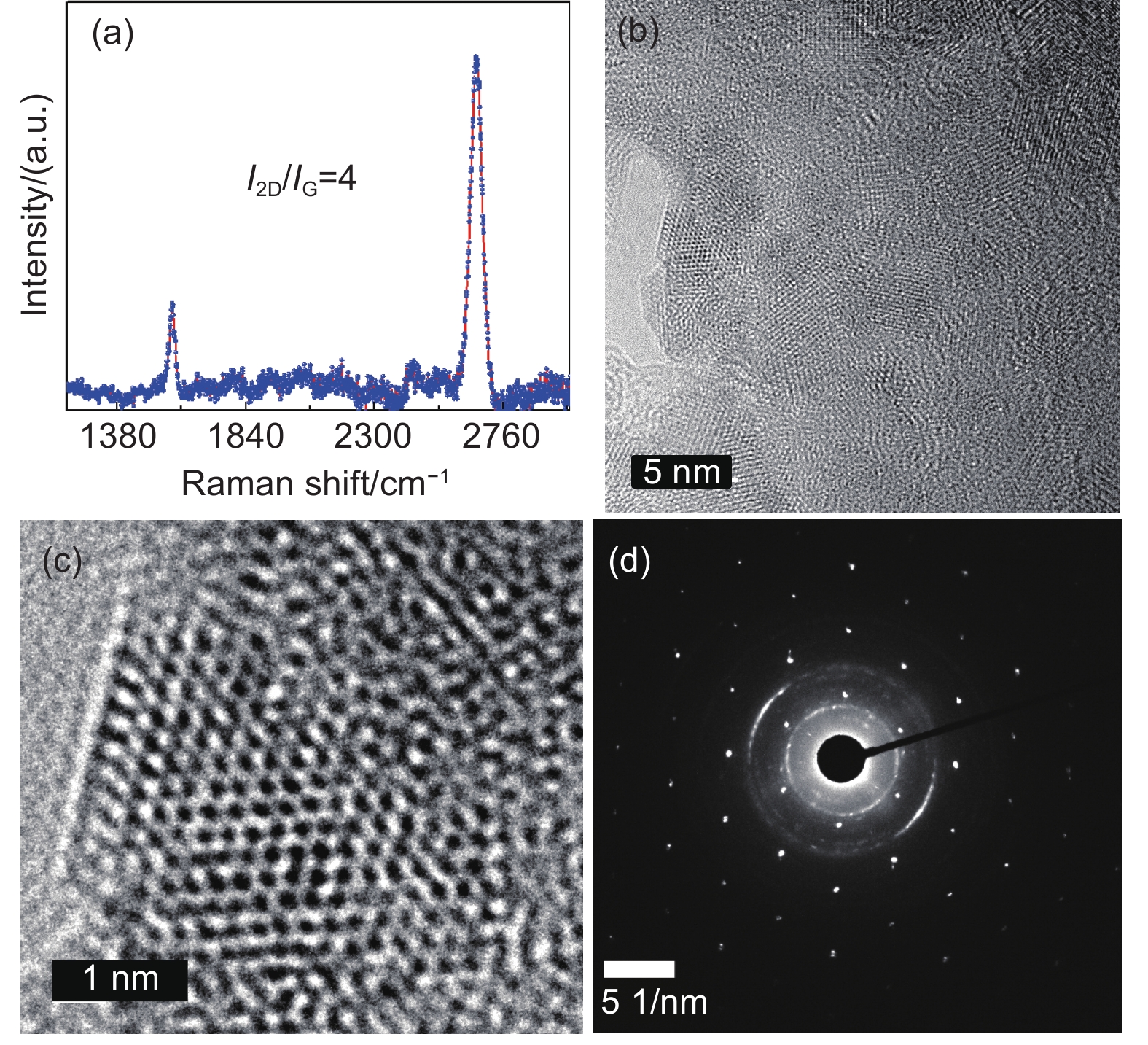
Figure 3. (a) Stacked Raman spectra of Ar-70, Ar-80 and Ar-100 with the I2D/IG ratio. (b, c, d) G-band (ωG), 2D-band (ω2D), and native oxide Raman spectra for Ar-70. (e, g) and (f, h) is the G- and 2D-band spectra for Ar-80 and Ar-100, respectively. The G-band position, 2D-band position, and FWHM (ωFWHM) are in cm−1

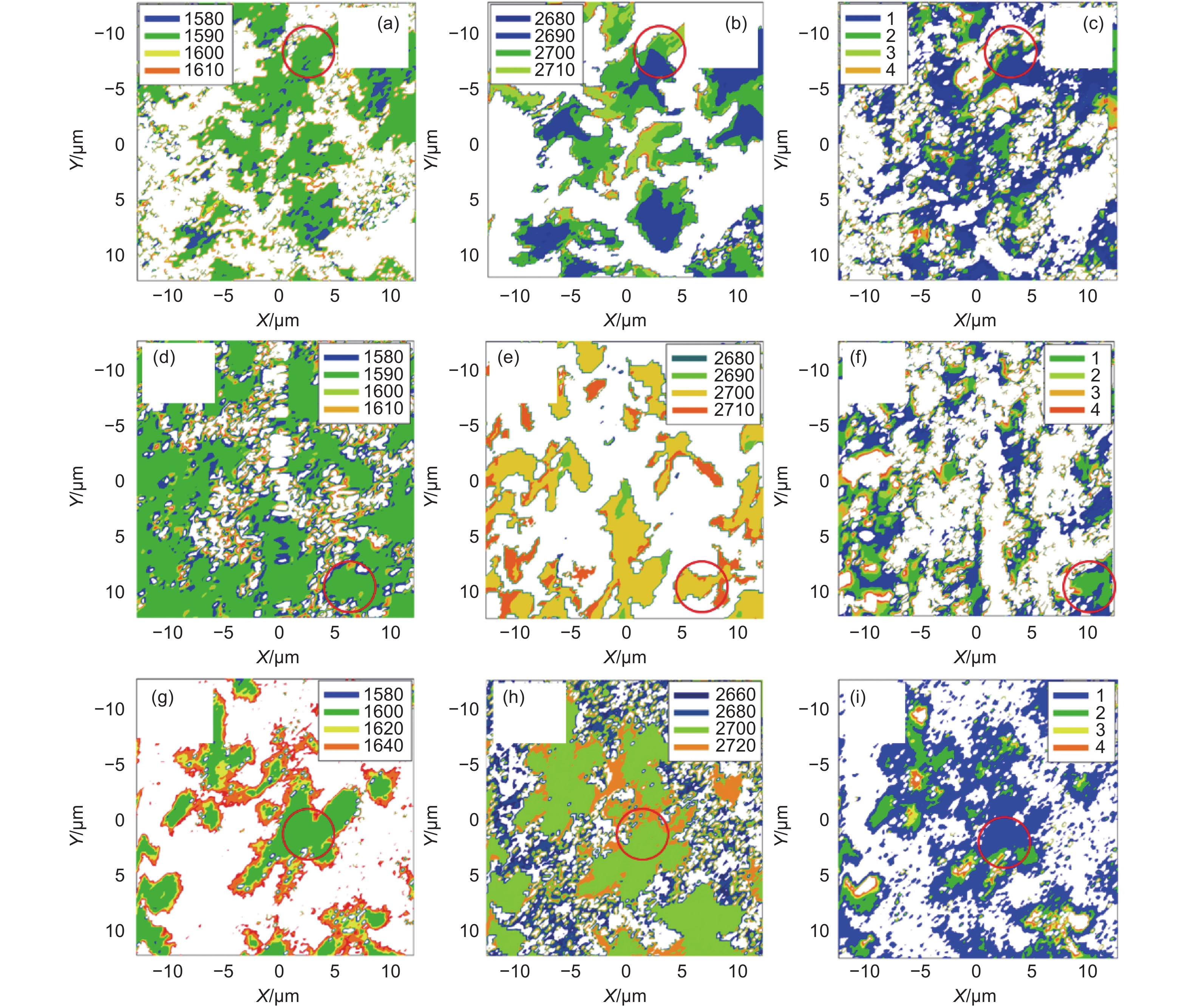
Figure 4. Two-dimensional plots of Raman mapping of (a, d, g) G-band, (b, e, h) 2D-band, and (c, f, i) I2D/IG ratio for Ar-70, Ar-80 and Ar-100, respectively

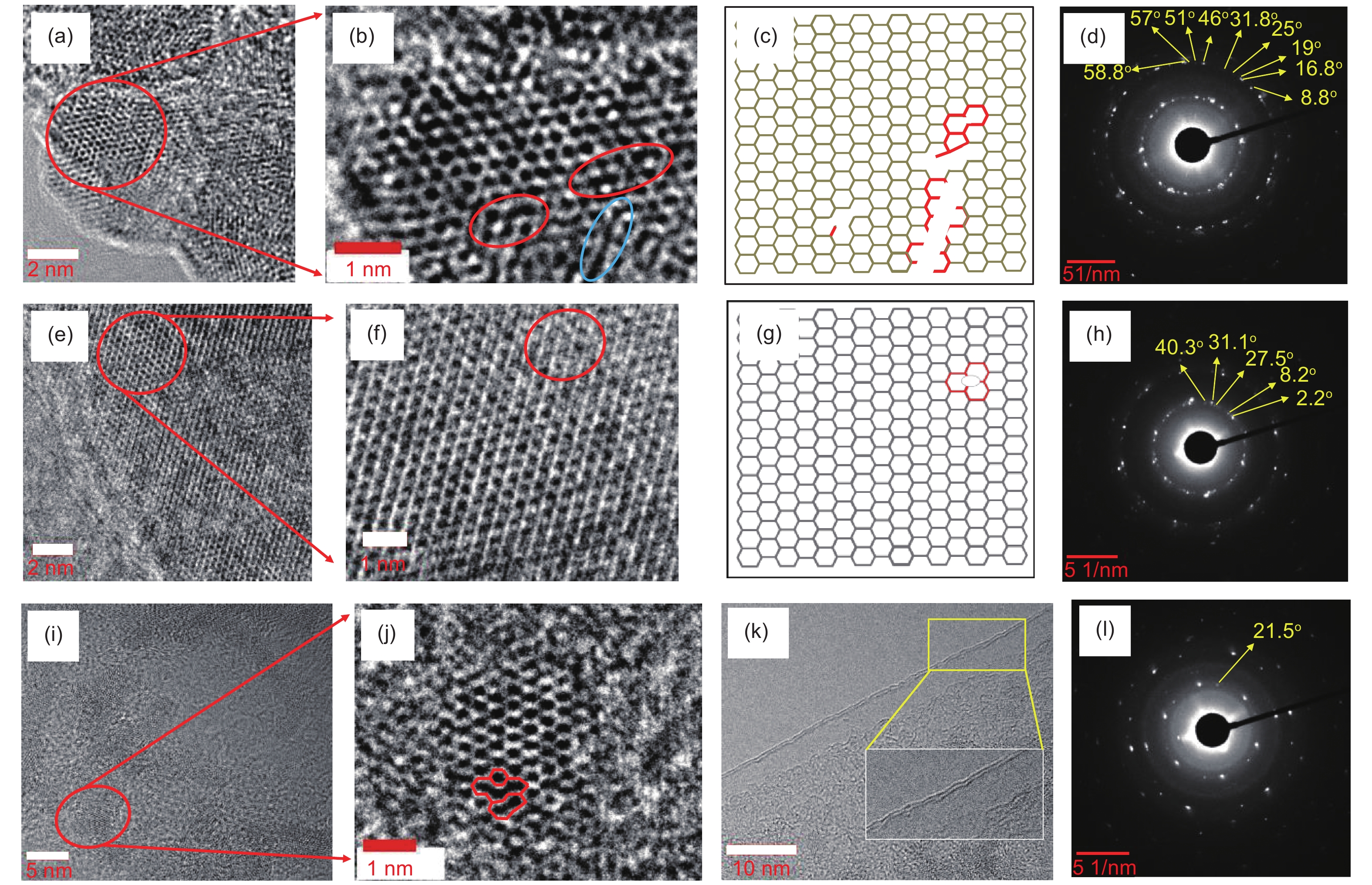
Figure 5. (a, b) High-resolution TEM images, (c) schematic of graphene lattice with defects, and (d) SAED pattern of Ar-70. (e, f) High-resolution TEM images, (g) schematic of graphene lattice with defects, and (h) SAED pattern of Ar-80. (i, j) High-resolution TEM images, (k) BLG edges, and (l) SAED pattern of Ar-100

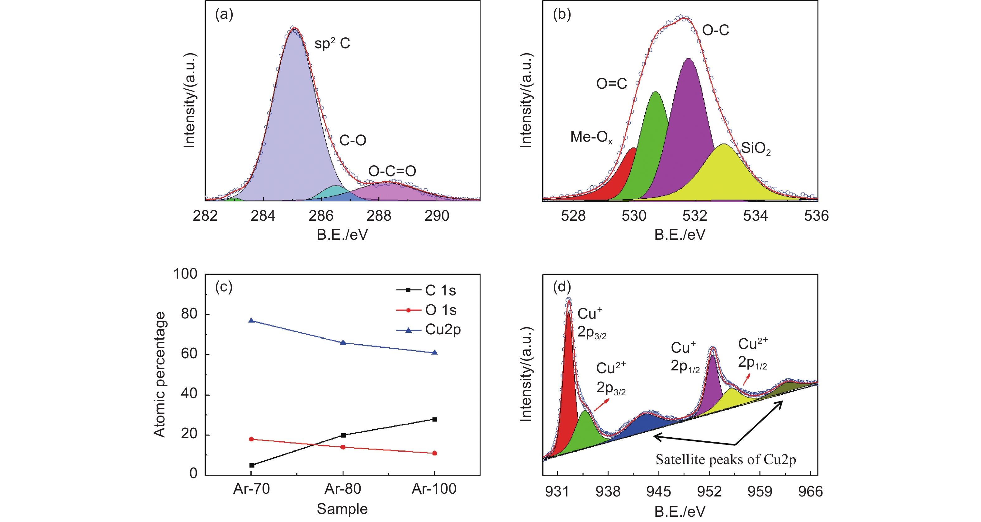
Figure 6. High-resolution XPS spectra of (a) C1s, (b) O1s of Ar-100 sample, (c) atomic percentage comparison of C1s, O1s, and Cu2p, and (d) spectra of Cu2p

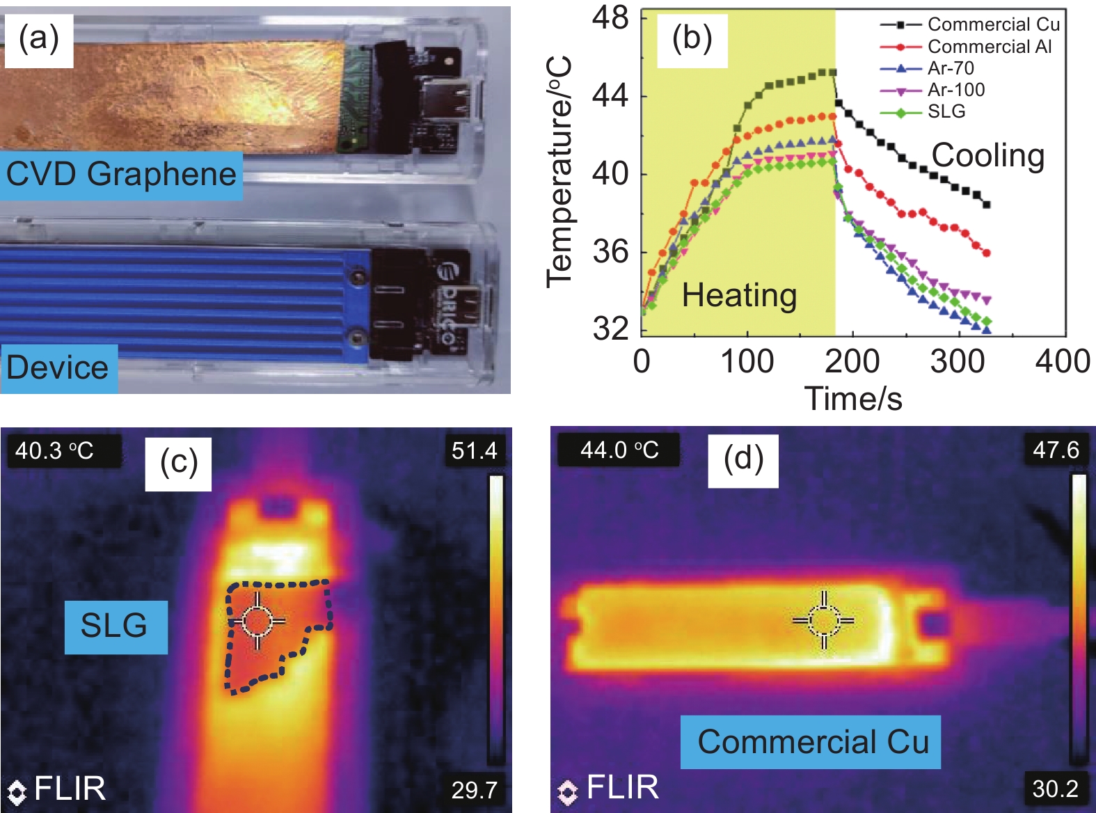
Figure 8. (a) Photographs of 2 TB SSD (108 (L) mm×34 (w) mm×11.5 (H) mm) with RTP-CVD graphene and commercial aluminium heat sink. (b) Temperature versus time profile of various heat sinks. Demonstration photographs of (c) a thermal IR camera with SLG and (d) commercial copper heat sink
-
[1] Kercher D S, Lee J B, Brand O, et al. Microjet cooling devices for thermal management of electronics[J]. IEEE Transactions on Components, Packaging and Manufacturing Technology,2003,26:359-366. doi: 10.1109/TCAPT.2003.815116 [2] Molina-Jordá J M. Nano- and micro-/meso-scale engineered magnesium/diamond composites: Novel materials for emerging challenges in thermal management[J]. Acta Materialia,2015,96:101-110. doi: 10.1016/j.actamat.2015.06.003 [3] Li H L, Wu X, Cheng K, et al. One-pot modified “grafting-welding” preparation of graphene/ polyimide carbon films for superior thermal management[J]. New Carbon Materials,2021,36:949-960. doi: 10.1016/S1872-5805(21)60076-8 [4] Chen J, Domingue J C, Sears C L. Microbiota dysbiosis in select human cancers: Evidence of association and causality[J]. Seminars in Immunology,2017,32:25-34. doi: 10.1016/j.smim.2017.08.001 [5] Balandin A A, Ghosh S, Bao W, et al. Superior thermal conductivity of single-layer graphene[J]. Nano Letters,2008,8:902-907. doi: 10.1021/nl0731872 [6] Li H L, Xiao S N, Yu H L, et al. A review of graphene-based films for heat dissipation[J]. New Carbon Materials,2021,36:897-910. doi: 10.1016/S1872-5805(21)60092-6 [7] Dong Z J, Sun B, Zhu H, et al. A review of aligned carbon nanotube arrays and carbon/carbon composites: fabrication, thermal conduction properties and applications in thermal management[J]. New Carbon Materials,2021,36:873-896. doi: 10.1016/S1872-5805(21)60090-2 [8] Lindsay L, Broido D A, Mingo N. Flexural phonons and thermal transport in graphene[J]. Physical Review B,2010,82:2-7. [9] Stankovich S, Dikin D A, Piner R D, et al. Synthesis of graphene-based nanosheets via chemical reduction of exfoliated graphite oxide[J]. Carbon,2007,45:1558-1565. doi: 10.1016/j.carbon.2007.02.034 [10] Kim K S, Zhao Y, Jang H, et al. Large-scale pattern growth of graphene films for stretchable transparent electrodes[J]. Nature,2009,457:706-710. doi: 10.1038/nature07719 [11] Seah C M, Chai S P, Mohamed A R. Mechanisms of graphene growth by chemical vapour deposition on transition metals[J]. Carbon,2014,70:1-21. doi: 10.1016/j.carbon.2013.12.073 [12] Zhang L, Hou G, Zhai W, et al. Aluminum/graphene composites with enhanced heat-dissipation properties by in-situ reduction of graphene oxide on aluminum particles[J]. Journal of Alloys and Compounds,2018,748:854-860. doi: 10.1016/j.jallcom.2018.03.237 [13] Bin Kim C, Lee J, Cho J, et al. Thermal conductivity enhancement of reduced graphene oxide via chemical defect healing for efficient heat dissipation[J]. Carbon,2018,139:386-392. doi: 10.1016/j.carbon.2018.07.008 [14] Rho H, Jang Y S, Bae H, et al. Fanless, porous graphene-copper composite heat sink for micro devices[J]. Scientific Reports,2021,11:1-7. doi: 10.1038/s41598-020-79139-8 [15] Deokar G, Avila J, Razado-Colambo I, et al. Towards high quality CVD graphene growth and transfer[J]. Carbon,2015,89:82-92. doi: 10.1016/j.carbon.2015.03.017 [16] Papon R, Pierlot C, Sharma S, et al. Optimization of CVD parameters for graphene synthesis through design of experiments[J]. Physica Status Solidi (B):Basic Research,2017,254:1-7. [17] Ferrari A C, Basko D M. Raman spectroscopy as a versatile tool for studying the properties of graphene[J]. Nature Nanotechnology,2013,8:235-246. doi: 10.1038/nnano.2013.46 [18] Wahab H S, Ali S, Abdul Hussein A, et al. Synthesis and Characterization of Graphene by Raman Spectroscopy[J]. Journal of Materials Sciences and Applications,2015,1:130-135. [19] Ferrari A C. Raman spectroscopy of graphene and graphite: Disorder, electron-phonon coupling, doping and nonadiabatic effects[J]. Solid State Communication,2007,143:47-57. doi: 10.1016/j.ssc.2007.03.052 [20] Lin Y C, Lu C C, Yeh C H, et al. Graphene annealing: How clean can it be?[J]. Nano Letters,2012,12:414-419. doi: 10.1021/nl203733r [21] Vlassiouk I, Smirnov S. Graphene nucleation density on copper: fundamental role of background pressure[J]. The Journal of Physical Chemistry A,2013,117:18919-18926. doi: 10.1021/jp4047648 [22] Riikonen S, Krasheninnikov A V, Halonen L, et al. The role of stable and mobile carbon adspecies in copper-promoted graphene growth[J]. The Journal of Physical Chemistry C,2012,116:5802-5809. doi: 10.1021/jp211818s [23] Muñoz R, Gómez-Aleixandre C. Review of CVD synthesis of graphene[J]. Chemical Vapor Deposition,2013,19:297-322. doi: 10.1002/cvde.201300051 [24] Zhang X, Guo X, Sun X, et al. Roles of CuO and Cu2O in graphene growth on a copper substrate[J]. Applied Surface Science,2022,576:151812. doi: 10.1016/j.apsusc.2021.151812 [25] Sahai A, Goswami N, Kaushik S D, et al. Cu/Cu2O/CuO nanoparticles: Novel synthesis by exploding wire technique and extensive characterization[J]. Applied Surface Science,2016,390:974-983. doi: 10.1016/j.apsusc.2016.09.005 [26] Gan Z H, Yu G Q, Tay B K, et al. Preparation and characterization of copper oxide thin films deposited by filtered cathodic vacuum arc[J]. Journal of Physics D:Applied Physics,2004,37:81-85. doi: 10.1088/0022-3727/37/1/013 -
 Supporting Information2022-0087.pdf

-


 下载:
下载:

 点击查看大图

计量
- 文章访问数: 249
- HTML全文浏览量: 135
- PDF下载量: 81
- 被引次数: 0